



Objective
PCB panelization is one of the most practical ways to reduce manufacturing costs without changing the actual circuit design. Instead of producing one board at a time, manufacturers place multiple boards on a larger production panel. That panel then moves through fabrication, assembly, inspection, and depanelization as one controlled unit.
This matters because many PCB production costs are attached to the panel, not only to the individual board. Every panel passes through drilling, plating, imaging, solder mask, routing, SMT assembly, AOI, testing, handling, and packing. When more usable boards fit on one panel, those fixed process costs are spread across more finished units.
Smart panelization does more than reduce material waste. It can improve SMT assembly efficiency, reduce handling, support better yield, and lower the final per-board cost. Poor panelization does the opposite. It can increase waste, create warpage, slow assembly, damage flex areas, and make depanelization harder.
For rigid, flex, and rigid-flex PCBs, the right panel layout must match both the design and the manufacturer’s process capability. A good manufacturer does not simply accept every customer-made panel. They review the layout, propose improvements, and provide working panel Gerber files for customer review when needed.
Key Takeaways
- PCB panelization places multiple boards on one production panel so they can be processed together.
- Good PCB panel size planning helps reduce material waste and lower per-unit cost.
- Panelization saves money during fabrication, SMT assembly, inspection, handling, and shipping.
- Rigid, flex, and rigid-flex boards need different panelization and depanelization planning.
- V-scoring works best for straight rigid boards, while routed tabs are better for irregular shapes.
- Flex and rigid-flex panels may need carriers, breakaway rails, stiffeners, or custom fixtures.
- Poor panel design can cause warpage, twisting, solder defects, edge damage, and low yield.
- Manufacturers like PCB Runner often propose optimized panel layouts based on real production capability.
 What Is PCB Panelisation?
Under PCB manufacturing, the correct usage and utilisation of raw materials is a key objective. To achieve this, PCB manufacturers use panelization strategies to determine the optimum number of boards that can fit within an array or production panel. This helps maximise material utilisation and allows manufacturers to offer more competitive pricing for both standard and HDI PCBs by increasing the number of boards produced from each panel.
PCB panelization is the process of repeating a PCB design within a larger production panel using the most suitable routing or depanelization method. This approach improves fabrication, assembly, inspection, and handling efficiency throughout production.
Panelization is used across many types of printed circuit board (PCB) manufacturing, including rigid PCBs, flex PCBs, rigid-flex PCBs, HDI boards, and mixed-technology boards. It is a critical manufacturing process because it directly affects cost, yield, quality, handling efficiency, and lead time throughout the PCB manufacturing process.
A good panel is not just a group of boards placed together. It is a manufacturing tool. It must support material utilisation, machine transport, SMT alignment, soldering, testing, and clean board separation.
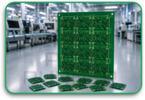
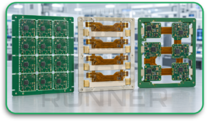
PCB Panelization For All Types Of PCBs: Rigid, Flex And Rigid-Flex
PCB panelization applies to rigid, flex, and rigid-flex PCBs, but the design approach is not the same for every board type.
Rigid PCBs are usually the easiest to panelise because the board structure is stable. They can often use V-scoring, tab routing, or solid tab routing depending on the outline and component placement. Rectangular rigid boards are often the most cost-efficient because they nest neatly into panels.
Flex PCBs need more careful support. A flexible circuit can bend, shift, or wrinkle during handling and assembly. For this reason, flex PCB panels may need temporary carriers, frames, stiffeners, adhesive support, or special fixtures. The goal is to keep the flex circuit flat and stable during printing, placement, soldering, and inspection.
Rigid-flex PCBs need even more planning. They combine rigid sections and flexible sections in the same board. The panel must protect bend areas while keeping rigid areas stable for assembly. Depanelization must not damage the flex arms, coverlay, stiffeners, or transition zones.
Semi-flex PCBs also need special care because the flexing region may be thinner or mechanically different from the rest of the board. The panel should support the board without creating stress in the flexible area.
A panelization method that works for a simple rigid board may not be safe for a flex or rigid-flex design. That is why panel layout should be reviewed with the manufacturer before production.
 Why PCB Panelization Is Used In Manufacturing
PCB panelization is used because it makes production more efficient. It allows several boards to move through manufacturing as one larger unit.
During fabrication, one panel can go through drilling, plating, imaging, etching, solder mask, silkscreen, surface finish, routing, and inspection. During assembly, the same panel can pass through stencil printing, pick-and-place, reflow soldering, AOI, X-ray inspection, and testing.
This reduces repeated handling and helps machines run more efficiently.
Panelization also improves stability. Small boards can be difficult for machines to transport. A larger panel with proper rails, fiducials, and tooling holes gives the assembly line a stable shape to grip, align, and process.
For high-volume production, panelization is essential. Without it, the cost per board would usually be much higher because every small board would need to be handled, aligned, processed, inspected, and packed separately.
Panelization is also useful for prototypes and small batches. Even 10 or 20 boards may be cheaper and easier to produce when grouped in a panel, especially if SMT assembly is required.
PCB Panelization vs Individual Board Production
Individual board production means each board is made and processed separately. This can work for very small one-off builds, engineering samples, or unusual designs that cannot be panelised easily. But it is usually inefficient for repeat production.
Panelised production groups multiple boards together. The panel moves through production as one unit, then the boards are separated later. This improves machine efficiency and reduces repeated setup, handling, and inspection effort.
The difference becomes clear during assembly. If one panel holds 20 boards, stencil printing happens once for 20 boards. Reflow happens once for 20 boards. Panel-level handling happens once for 20 boards. If those same boards are processed individually, the line has to handle many more separate units.
Panelised production also helps maintain consistency. Boards on the same panel usually experience the same process conditions. This supports better repeatability compared with handling many loose small boards.
Individual production may still be used for special cases, but panelization is usually the better choice when cost, yield, speed, and repeatability matter.
Why Panelization Is A Cost-Saving Strategy In PCB Manufacturing
Panelization reduces cost because it improves how material, machines, labour, and time are used. The savings do not come from one place only. They build up across fabrication, assembly, inspection, handling, and shipping.
A well-planned PCB panel size can fit more boards into the same manufacturing run. This means the fixed cost of processing one panel is divided across more finished boards.
However, bigger is not always better. An oversized panel can warp during reflow soldering, while an excessively thin panel may twist during processing. Poor board arrangement can also lead to material waste or create weak breakaway points.
The goal is not to make the biggest panel possible. The goal is to make the most efficient panel that the manufacturer can process reliably.
Improved Material Utilisation
Material utilisation means how much of the panel area becomes usable finished boards. If a panel has too much empty space, the OEM is paying for laminate that becomes scrap.
Good board arrangement improves material utilisation. Rectangular boards are usually easier to nest. Irregular outlines may leave unused gaps unless the layout is carefully rotated or arranged.
For flex and rigid-flex PCBs, material utilisation must be balanced with support needs. A flex panel may need carrier areas, rails, or handling frames. These areas use material, but they may be necessary for yield and process stability.
The lowest material waste is not always the lowest total cost. If a tightly packed panel causes assembly or depanelization damage, the saving is lost through scrap and rework.
Reduced Production Handling
Handling costs are easy to overlook. Every time a board is picked up, loaded, aligned, inspected, moved, counted, packed, or shipped, time and risk are involved.
Panelization reduces handling because multiple boards move together. Operators and machines handle one panel instead of many small pieces.
This is especially important for small boards, thin boards, flex circuits, and rigid-flex designs. Loose flex circuits can bend or shift during handling. Panel support helps keep them stable until assembly is complete.
Reduced handling also lowers the chance of scratches, edge damage, contamination, broken tabs, bent flex arms, and misplaced parts.
Better Manufacturing Efficiency And Yield
Good panelization improves manufacturing efficiency. Machines can process more boards per pass, and operators spend less time loading, aligning, and moving individual units.
Yield can also improve when the panel is stable. A well-supported panel reduces warpage, twisting, solder paste misalignment, component placement errors, and handling damage.
For SMT assembly, a stable panel helps the solder paste printer, pick-and-place machine, and reflow oven work consistently.During inspection, AOI and X-ray systems can scan boards more efficiently when they remain in panel form.
Yield for flex and rigid-flex boards depends heavily on proper support throughout the manufacturing process. A poor panel can allow movement during stencil printing or placement. This can cause paste defects, shifted components, and soldering issues.
Lower Per-Unit Manufacturing Costs
Panelization lowers per-unit manufacturing costs by spreading fixed process costs across more boards.
Setup, machine programming, stencil printing, conveyor handling, reflow, AOI setup, testing preparation, and internal logistics are often more efficient at panel level. The more usable boards on a reliable panel, the lower the cost per finished board usually becomes.
The final saving depends on board size, component count, routing time, inspection needs, panel size, test requirements, and manufacturer capability.
Smart panelization is not only about fitting more boards. It is about fitting the right number of boards in a panel that can be produced with good yield and safe handling.
Types Of Depanelization In PCB Panels
Depanelization is the process of separating individual boards from the production panel. The right method depends on board type, board outline, material, thickness, component location, flex areas, edge quality, and mechanical stress limits.
For rigid PCBs, common methods include V-scoring, tab routing, perforated tabs, solid tabs, mechanical routing, and punching. For flex and rigid-flex PCBs, the depanelization method must be chosen more carefully because bending, tearing, or edge stress can damage the circuit.
V-Scoring (V-Cut)
V-scoring uses a V-shaped groove cut along straight separation lines. The groove is made on one or both sides of the panel so the boards can be separated after assembly.
V-scoring works best for rigid PCBs with straight rectangular outlines. It is fast and cost-effective when boards are arranged in rows or arrays.
For flex PCBs, V-scoring is usually not the preferred method because flexible material does not snap like rigid laminate. For rigid-flex PCBs, V-scoring may be used only in rigid sections if the design allows it. It should not create stress near flex transition areas.
V-scoring is not suitable for curved edges or irregular outlines. It also requires enough clearance from components near the board edge.
Tab Routing
Tab routing uses a router to cut around the board outline while leaving small tabs that hold each board in the panel. The tabs are removed after assembly.
This method works well for irregular board shapes, cutouts, and boards that cannot use V-scoring. It is common in rigid PCB panelization and can also be used with rigid-flex boards when the tabs are placed in safe rigid areas.
For flex boards, tab routing must be planned carefully. Tabs should not stress the flexible circuit or cause tearing during removal. Temporary support frames or carriers may be needed.
Tab routing gives more shape flexibility than V-scoring, but it can take more routing time and may leave small edge marks after separation.
Perforated Tab Routing
Perforated tab routing, often called mousebite tab routing, uses small drilled holes along the tab. These holes weaken the tab so the board can be broken away more easily.
This method is useful for many rigid PCBs with irregular shapes. It allows easier manual separation compared with solid tabs.
However, mousebites can leave small bumps on the board edge. This may be acceptable for many applications, but not for boards that require smooth edges, sliding fit, tight enclosure tolerance, or edge connectors.
For flex and rigid-flex PCBs, perforated tabs must be used with caution. Breaking the tab manually can create stress. Tabs should be placed away from flex regions, bend zones, and sensitive edge features.
Solid Tab Routing
Solid tab routing uses connecting tabs without mousebite holes. The tabs are stronger and provide better support during assembly. After assembly, the tabs are removed using a depaneling machine, router, blade, or other controlled process.
Solid tabs are useful when the panel needs stronger support during SMT assembly or when the board edge needs to be cleaner than mousebite separation allows.
For rigid-flex and flex assemblies, solid tabs may help reduce movement during processing. However, removal must be controlled carefully to avoid bending or tearing the flexible section.
Solid tab routing often costs more than simple V-scoring or mousebite tabs, but it can improve quality for sensitive designs.
Micro Dicing
Micro dicing uses a precise cutting process to separate small or delicate boards. It can be useful where edge quality, dimensional control, or low mechanical stress is important.
This method may be used for thin boards, small modules, ceramic-like substrates, or applications where the board edge must remain clean and controlled.
For flex and rigid-flex boards, micro dicing may be considered when standard mechanical separation creates too much stress. The method depends on the material set, board thickness, copper layout, and manufacturer capability.
Micro dicing is not always needed, but it can support high-precision applications where standard routing or snapping methods are too rough.
Individual Through Mechanical Routing, Laser, Or Fixture Punch
Some boards are separated individually through mechanical routing, laser cutting, or fixture punching.
Mechanical routing is common for rigid PCBs and some rigid-flex panels. It can follow irregular outlines and produce controlled board edges. The tradeoff is routing time and tool wear.
Laser cutting may be used for certain flex and thin materials where mechanical stress must be reduced. It can produce accurate cuts, but the material, edge quality, and thermal effects must be reviewed.
Fixture punching uses a custom tool to separate boards quickly. It can be efficient for high volumes, but the tooling cost must be justified. It is usually more suitable when the design is stable and production volume is high.
For flex and rigid-flex PCBs, the separation process should always protect bend areas, coverlay edges, stiffeners, exposed conductors, and transition zones.
How PCB Arrangement In Panel Affects Material Utilisation And Waste Reduction
The way boards are arranged in a panel has a direct impact on material waste and total cost.
If boards are placed with large gaps, too much laminate is wasted. If they are placed too close, routing tools, V-score blades, components, or depanelization equipment may not have enough clearance.
Board rotation can also affect material use. Sometimes rotating a board by 90 degrees allows more pieces to fit in the same panel. For irregular shapes, nesting can reduce unused gaps.
Tooling rails, breakaway rails, fiducials, coupon areas, routing channels, and tab locations also take space. These areas are necessary, but they do not become finished boards. A good panel balances usable board count with required manufacturing support.
For flex and rigid-flex panels, waste reduction must be balanced with process stability. Extra support material may look wasteful, but it can prevent movement, warpage, and handling damage. In many cases, a slightly less dense panel with better support gives a better total cost because yield improves.
Panelization And Its Impact On SMT Assembly Process Efficiency
Panelization has a major impact on SMT assembly efficiency. An SMT line processes panels through solder paste printing, pick-and-place, reflow soldering, and inspection.
Solder paste printing happens at the panel level. A stable panel allows the stencil to align correctly and deposit paste accurately. If the panel flexes or twists, paste deposits may shift or smear.
Pick-and-place machines also benefit from stable panels. The machine uses fiducials to align the panel and place components accurately. If the panel is poorly supported, placement accuracy can suffer.
Reflow soldering depends on thermal consistency. A poorly designed panel may heat unevenly or warp in the oven. Warpage can cause tombstoning, solder bridges, opens, and component misalignment.
AOI is also more efficient when boards are inspected in panel form. Setup and handling are reduced, and inspection can move across the panel in a controlled way.
For flex and rigid-flex boards, SMT efficiency depends on carriers, stiffeners, rails, and fixtures. Without proper support, flexible areas can move during printing or placement. This can reduce yield and increase rework.
Fiducial Marks, Tooling Holes, And Panel Breakaway Rails Explained
Fiducial marks, tooling holes, and breakaway rails help the panel move accurately through fabrication and assembly.
SMT machines use fiducial marks as reference points for precise alignment during assembly. Panel-level fiducials help the machine locate the whole panel. Local fiducials may be used near fine-pitch ICs, BGAs, or dense component areas.
Tooling holes help with mechanical alignment, fixture location, testing, or handling. They must be placed where they do not interfere with components, routing, flex areas, or depanelization paths.
Breakaway rails are extra panel material around the board array. They help conveyors grip and transport the panel through SMT equipment. Rails may also hold fiducials, tooling holes, barcodes, coupons, or handling features.
Breakaway rails are often straightforward for rigid PCBs. Flex PCBs, however, may require rails or carriers to keep the flexible circuit flat during processing. In rigid-flex PCBs, the rails should support the rigid sections without placing stress on flex arms or bend zones.
These features use panel space, but they are often necessary for efficient assembly and better yield.
PCB Panelization Design Rules And Best Practices
Good PCB panelization starts with manufacturing capability. Panel design should match the equipment, process limits, material type, board thickness, and assembly method.
Keep inter-board spacing consistent. Confirm the spacing with the manufacturer because the required gap depends on separation method, router bit size, V-score clearance, board thickness, component overhang, and handling requirements.
Place tabs where they support the board without stressing sensitive areas. Avoid placing tabs near connectors, edge contacts, fine traces, RF edges, flex bends, or rigid-flex transition zones.
Check component overhang. Some connectors, capacitors, switches, and mechanical parts may extend beyond the board edge. The panel must give them enough clearance during assembly and depanelisation.
Use panel-level fiducials for SMT alignment. Add local fiducials where fine-pitch placement requires higher accuracy.
Avoid panel sizes that are too large for the board thickness and construction. Thin panels can warp during reflow. Rigid-flex panels can twist if support is not balanced.
For flex PCBs, keep the circuit supported during assembly. Use carriers, frames, or fixtures where required. Avoid panel designs that allow flex tails to flap or bend during processing.
For rigid-flex PCBs, protect the bend areas. Do not place tabs, break lines, stress points, or hard tooling features near flex-to-rigid transitions.
Run a DFM review before release. Panelization should be checked before Gerber files are finalized.
How Panelization Reduces Per-Unit Assembly Costs
Panelization reduces per-unit assembly costs by improving line efficiency.
Stencil printing, panel loading, conveyor movement, reflow, AOI, and many handling steps happen at the panel level. If the panel carries more boards, these costs are spread across more finished units.
Pick-and-place time still depends on the total number of components, but setup and handling become more efficient when boards are panelised.
Testing and inspection can also become more efficient. AOI can scan the panel in one program. Electrical testing may use panel-level fixtures. Operators can track and handle groups of boards instead of individual pieces.
Per-unit cost drops when panelization increases board count without increasing defects, rework, warpage, or depanelization damage.
That last point matters. A panel that fits more boards but causes lower yield is not cheaper. True savings come from an optimized panel that supports both efficiency and reliability.
Mistakes To Avoid When Designing Panels For Production
One common mistake is designing a panel size that the manufacturer cannot run efficiently. Every manufacturer has preferred panel sizes and equipment limits. Non-standard sizes may increase cost or require extra handling.
Another mistake is placing boards too close together. Routing tools, V-score blades, tabs, component overhangs, and depanelization equipment need clearance.
Placing boards too far apart is also a problem. Extra spacing wastes material and increases PCB panel size cost without improving quality.
Choosing the wrong separation method can also add cost. V-scoring is efficient for straight rigid boards, but it is not suitable for irregular shapes. Tab routing works for more complex outlines but can leave edge nubs. Flex and rigid-flex boards may need special support and controlled separation.
Another mistake is forgetting component overhang. If parts extend beyond the board edge, nearby boards may interfere during SMT assembly or handling.
For flex PCBs, a major mistake is allowing the flex circuit to move during assembly. Unsupported flex can shift during paste printing, placement, or reflow.
For rigid-flex PCBs, avoid placing tabs or breakaway stress points near bend areas or rigid-flex transitions. This can damage the flexible section or shorten product life.
Skipping manufacturer review is another expensive mistake. A design that looks efficient in CAD may not suit real manufacturing conditions.
Working With Your PCB Manufacturer To Optimize Panel Layout
A customer-made panel is not always accepted as-is by a reputable manufacturer. In many cases, the manufacturer will review the files and propose a better panel layout based on actual production capability.
This is not done to complicate the project. It is done to improve yield, avoid warpage, prevent twisting, reduce handling problems, and match the manufacturer’s equipment.
A reputable manufacturer like PCB Runner may propose the panel layout and provide working panel Gerber files or panel drawings for customer review. This allows the end customer to confirm the production panel before manufacturing begins.
The manufacturer considers panel size, board arrangement, material utilization, routing paths, breakaway rails, tooling holes, fiducials, tab placement, component overhang, board thickness, flex support, rigid-flex transition areas, and depanelization method.
For rigid boards, this may mean changing the array size, rotating boards, adjusting spacing, or using V-score instead of tab routing.
For flex and rigid-flex boards, it may mean adding carriers, support rails, stiffener planning, controlled tabs, or special depanelization methods.
Working with the manufacturer early helps reduce cost, improve quality, and avoid delays. It also ensures the final panel is designed for real production, not only for drawing convenience.
Conclusion
Smart PCB panelization reduces total cost by improving material use, production handling, SMT assembly efficiency, inspection flow, and yield. It also helps reduce lead time because fewer individual boards need to be handled through each process step.
The best panel is not always the panel that fits the most boards. The best panel is the one that fits the right number of boards while staying stable, manufacturable, easy to assemble, and safe to depanel.
Rigid, flex, and rigid-flex PCBs each need different panelization planning. Flex and rigid-flex designs often need more support, more careful tab placement, and special depanelization methods to avoid stress or damage.
Working with PCB Runner early helps ensure the panel layout matches real manufacturing capability. With the right panel size, board arrangement, breakaway method, fiducials, tooling holes, and support features, OEMs can reduce PCB panel size cost, improve yield, and shorten production lead time.
FAQs
What Is PCB Panelisation?
PCB panelization is the process of arranging multiple individual PCBs on one larger production panel. The panel moves through fabrication, assembly, inspection, and testing before the boards are separated.
Why Is PCB Panelization Used In Manufacturing?
PCB panelization is used to improve material use, reduce handling, increase assembly efficiency, improve yield, and lower the cost per finished board.
Does PCB Panelization Apply To Flex And Rigid-Flex PCBs?
Yes. Flex and rigid-flex PCBs can be panelised, but they need more careful support, fixturing, and depanelization planning than standard rigid boards.
How Does PCB Panel Size Affect Cost?
PCB panel size affects how many boards fit in one production run. A well-optimized panel spreads fixed process costs across more boards and reduces material waste.
Is A Larger PCB Panel Always Cheaper?
No. Larger panels can reduce per-unit cost, but panels that are too large may warp, twist, or reduce yield. The best panel size depends on board design and manufacturer’s capability.
What Is The Difference Between V-Scoring And Tab Routing?
V-scoring cuts straight grooves so boards can be snapped apart. Tab routing cuts around the board outline and leaves tabs to hold the board in place. V-scoring is best for straight rigid boards, while tab routing works better for irregular shapes.
Are Mousebite Tabs Suitable For Every PCB?
No. Mousebite tabs are useful for many rigid boards, but they can leave edge nubs. They may not be suitable for boards needing smooth edges, tight mechanical fit, or sensitive flex areas.
Why Are Fiducials Needed In PCB Panels?
Fiducials help SMT machines align the panel accurately. Panel-level fiducials support overall alignment, while local fiducials help with fine-pitch components and dense areas.
Can A Manufacturer Change A Customer-Made Panel?
Yes. A reputable manufacturer may propose a better panel layout to improve yield, reduce warpage, support assembly, and match their equipment capability. The revised panel can be shared with the customer for review.
How Does Panelization Reduce Assembly Cost?
Panelization reduces assembly cost by allowing multiple boards to pass through stencil printing, pick-and-place, reflow, AOI, and handling as one panel. This spreads process costs across more finished units.



