A great PCB design means nothing if it cannot be manufactured reliably, and that is exactly what DFM solves.
Most production delays and cost overruns in electronics do not come from bad ideas. They come from designs that were never reviewed for how they would actually be built. Research from the IPC consistently shows that design-related issues cause the majority of PCB manufacturing defects. PCB manufacturing problems caught at the design stage cost a fraction of what they cost when discovered during production or after delivery.
PCB Runner sees this pattern regularly, good engineers, solid designs, but no DFM process. The result is delays, scrap, and expensive respins. This guide explains DFM clearly, practically, and in a way that is useful whether you are building your prototype or scaling to mass production.
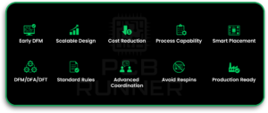
Key Takeaways
- DFM should start during the PCB design stage, not after the layout is complete.
- A PCB can work well as a prototype but still fail when production scales if manufacturability is not checked early.
- Good DFM reduces production delays, scrap, rework, and unnecessary cost.
- Trace width, spacing, pad size, drill size, annular rings, and layer stack-up must match the manufacturer’s real process capability.
- Component placement affects assembly speed, soldering quality, inspection, and rework access.
- DFM, DFA, and DFT work together. A board should be easy to fabricate, assemble, and test.
- Using standard components, proven footprints, and manufacturer-approved design rules makes production smoother.
- High-speed and multilayer PCBs need closer coordination with the fabricator because signal integrity, impedance, thermal control, and stack-up choices are more sensitive.
- Ignoring manufacturer guidelines often leads to engineering queries, production stops, failed boards, or expensive respins.
- DFM is not extra work. It is the step that helps a PCB move from design to scalable production with fewer surprises.
What Is Design for Manufacturability (DFM) in PCB?
Simple Definition of DFM in Electronics Manufacturing
Design for Manufacturability, or DFM, is the process of designing a PCB to be manufactured efficiently, consistently, and without unnecessary complications. It is not about limiting creativity. It is about making sure your design works in a real factory, with real equipment, at real tolerances.
DFM asks one fundamental question at every design decision: Can this actually be built reliably?
Why DFM Is Critical for Scalable Production
A design that works for ten prototype boards may completely break down at five thousand units. Tolerances that a skilled technician handles manually in prototyping cannot be managed the same way in automated production. DFM closes that gap. It aligns your design intent with what manufacturing equipment and processes can consistently deliver.
Difference Between DFM, DFA, and DFT
These three terms are related but distinct:
- DFM (Design for Manufacturability): Focuses on making the board easy to fabricate, correct trace widths, drill sizes, spacing, and layer stack-up
- DFA (Design for Assembly): Focuses on making component placement and soldering efficient and error-free
- DFT (Design for Testing): Focuses on making sure the finished board can be tested thoroughly, test points, bed-of-nails access, boundary scan compatibility
All three work together. A board optimized for all three is significantly cheaper and faster to produce than one that ignores them.
Why DFM Matters in Modern PCB Production
Reducing Manufacturing Errors and Rework
Every error caught during design review costs almost nothing to fix. The same error caught during fabrication requires scrapping panels, reordering material, and restarting the build. Caught after assembly, it means desoldering components, reworking the board, and retesting, all of which add cost and time that no schedule has a budget for.
Improving Production Speed and Efficiency
A DFM-compliant design moves through fabrication and assembly without stops for engineering queries, tolerance exceptions, or process adjustments. Production lines run at full speed when the design is ready for them. Unreviewed designs cause constant interruptions.
Lowering Overall Production Costs
DFM reduces material waste, shortens cycle times, improves first-pass yield, and reduces the need for manual intervention. In high-volume PCB manufacturing, even a 2% improvement in yield can represent substantial cost savings across an entire production run.
How DFM Fits Into the PCB Development Process
Role of DFM During PCB Design Stage
DFM should begin during PCB design—not after. When a designer sets trace widths, chooses component packages, plans the layer stack-up, and defines pad sizes, each decision has a DFM implication. Fixing those decisions after the design is complete is far more disruptive than getting them right the first time.
Importance Before Prototype and Mass Production
The prototype stage is your last low-cost opportunity to catch DFM issues before they scale. A problem that appears on one prototype board will appear on every board in your production run. DFM review before prototyping prevents costly surprises from multiplying.
Collaboration Between Designers and Manufacturers
The most effective DFM happens when designers and manufacturers talk to each other early. Manufacturers know their equipment’s true capabilities, the minimum trace widths they can reliably hold, the drill tolerances they can guarantee, and the solder paste volumes that work with their stencils. Designers who access that information during layout make far better decisions than those who rely solely on generic design rules.
PCB Runner Guide To DFM Reviews
A DFM review checks whether a PCB design can move into production without avoidable problems. It looks beyond the electrical design and focuses on how the board will be fabricated, assembled, inspected, and tested.
PCB Runner reviews the design files, stack-up, drill data, Gerbers, BOM, assembly notes, and manufacturing requirements before production begins. This helps catch issues that may not appear in schematic or layout checks alone.
A proper DFM review can identify:
- Trace and spacing issues
- Incorrect pad sizes
- Tight drill tolerances
- Weak annular rings
- Poor component clearance
- Risky via choices
- Solder mask problems
- Assembly access concerns
- Missing or unclear fabrication notes
The value of a DFM review is simple. It helps correct small design issues before they become production delays, scrap, or expensive respins.
Core Principles of DFM in PCB Design
Simplifying PCB Layout for Easy Manufacturing
Complexity that does not serve a functional purpose creates manufacturing risk. Unnecessary microvias, exotic materials, non-standard pad shapes, and unusual stack-ups all increase the risk of errors and raise fabrication costs. Keep the PCB layout as simple as the design requirements allow.
Standardizing Components and Materials
Using components from a standardized library, with established land patterns and known assembly characteristics, reduces the chance of footprint errors and makes sourcing easier. Exotic or single-source components create supply chain risk that compounds at scale.
Designing for Consistent Production Output
A good DFM design produces the same result every time, not just most of the time. This means designing within your manufacturer’s process capabilities— not at the edge of them—so that normal process variation does not push boards out of specification.
Key DFM Guidelines Every PCB Designer Should Follow
Proper Trace Width and Spacing
Most fabricators can reliably produce traces and spaces of 0.1 mm (4 mil) or wider in standard processes. Pushing below this requires advanced fabrication capabilities and increases cost. Always check your manufacturer’s minimum trace and space specification before routing fine-pitch areas.
Correct Pad Sizes and Annular Rings
An annular ring is the copper remaining around a drilled via hole. IPC-2221 recommends a minimum annular ring of 0.05 mm for controlled impedance designs. Rings that are too small risk breakout, where the drill hole touches the edge of the pad, causing open circuits and failed boards.
Drill Size Optimization and Tolerance Management
Standard mechanical drilling handles holes of 0.2 mm and larger. Below that, laser drilling is required, which adds cost. Aspect ratio (board thickness divided by hole diameter) matters too. A 1.6 mm board with 0.2 mm holes has an aspect ratio of 8:1, near the limit for reliable plating. Stay within your fabricator’s stated capability.
Layer Stack-Up Planning for Manufacturability
The PCB layout process for multilayer boards must account for how prepreg and core materials combine to achieve controlled impedance. Stack-up must be defined in collaboration with the fabricator, not assumed. A stack-up that works in a simulation but cannot be built with standard laminate thicknesses will require expensive custom materials.
Component Placement Best Practices for DFM
Maintaining Adequate Spacing Between Components
IPC-7351 guides minimum component-to-component spacing. For standard SMT assembly, a minimum of 0.2 mm between component bodies is a reasonable floor. Tighter spacing interferes with solder paste printing, placement accuracy, and inspection access.
Orientation Consistency for Automated Assembly
Polarized components, capacitors, diodes, and ICs, should be oriented consistently across the board. When all polarized components share the same orientation pattern, automated optical inspection (AOI) runs faster and picks up errors more reliably. Random orientations slow down programming, placement, and inspection.
Avoiding Congested Areas on the Board
Dense component clusters create problems for solder paste stenciling, pick-and-place accuracy, and rework access. If a component is so tightly surrounded that a soldering iron cannot reach it for rework, that is a DFM failure. Always leave enough room for practical access.
Design Considerations for Soldering and Assembly
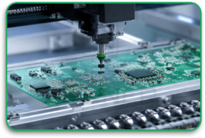
Designing for SMT Processes
Surface mount technology (SMT) is the dominant assembly process. For SMT compatibility:
- Use standard IPC-compliant land patterns for all SMT components
- Ensure thermal relief connections on power pads to prevent cold solder joints
- Avoid placing SMT components too close to board edges, where solder paste stencils lift
Through-Hole Component Placement Guidelines
Through-hole components require wave soldering or selective soldering, both of which have their own clearance requirements. Maintain at least 5 mm clearance between through-hole component bodies and nearby SMT components on the solder side to prevent shadowing during wave solder.
Avoiding Solder Bridges and Tombstoning Issues
Solder bridges form when two adjacent pads are unintentionally connected by solder. Adequate pad-to-pad spacing and correct solder mask dam widths (minimum 0.1 mm) prevent this. Tombstoning, where one end of a small passive component lifts during reflow, happens when pad sizes are asymmetric or thermal mass is unbalanced. Symmetrical pad design and correct stencil apertures prevent it.
Common DFM Issues That Cause Production Delays
- Tolerances tighter than fabricator capability, boards fail inspection, panels are scrapped
- Missing or incorrect Gerber data, production cannot start until the files are corrected
- Poor thermal layout, boards warp during reflow, components shift
- Incorrect drill-to-copper clearance, causes short circuits after drilling
- Non-standard component footprints, assembly errors and rework at scale
Common PCB DFM Failures Seen During Production
Many PCB production issues come from design choices that were not reviewed early enough. These problems may not look serious during layout, but they can create real trouble once boards enter fabrication or assembly.
Common PCB DFM failures include:
- Drill holes breaking out of pads
- Solder bridges between close pads
- Tombstoning on small passive parts
- Warping during reflow
- Poor solder flow around thermal pads
- Components placed too close together
- Missing solder mask dams
- Incorrect or outdated footprints
- Copper too close to the board edge
- Fine traces that exceed process capability
These failures slow production because the manufacturer has to stop, ask questions, adjust the process, or scrap boards. In larger runs, even a small repeat issue can become expensive very quickly.
A good DFM process helps catch these weak points before the board reaches the production floor.
PCB DFM Checklist Before Manufacturing
Before sending a PCB design for manufacturing, the files should be checked against the manufacturer’s real process limits. A board may pass basic design rule checks and still create problems during fabrication or assembly.
Use this checklist before releasing files:
- Confirm trace width and spacing match manufacturer limits
- Check pad sizes and annular rings
- Review drill sizes and aspect ratios
- Confirm copper-to-edge clearance
- Check solder mask openings
- Review silkscreen placement
- Confirm stack-up details
- Check component footprints
- Verify polarity markings
- Review spacing between components
- Add enough test points
- Confirm BOM accuracy
- Check panelization needs
- Run DRC and DFM checks
- Ask the manufacturer to review the files before production
This checklist gives the manufacturer cleaner files to work with. It also reduces engineering queries and helps production start with fewer delays.
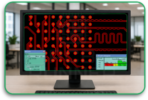
Tools and Checks Used for DFM Validation
Automated DFM Software Tools
Tools like Cadence Allegro, Altium Designer, and KiCad all include built-in DRC engines. Third-party platforms like Valor NPI and CAM350 perform more detailed DFM analysis specifically oriented toward fabrication and assembly process requirements.
Design Rule Checks (DRC) Explained
A DRC checks your layout against a set of rules, minimum trace width, minimum via size, clearance requirements, and copper-to-board-edge distances. Running DRC before sending files to a fabricator catches the most obvious errors. It does not replace the manufacturer’s DFM review, but it prevents wasting everyone’s time on basic mistakes.
Manufacturer DFM Feedback Reports
Most professionals provide a DFM feedback report after receiving your design files. This report flags issues that their equipment cannot handle, recommends changes, and sometimes offers alternative approaches. Read these reports carefully, they represent real manufacturing experience applied to your specific design.
How PCB Manufacturers Perform DFM Analysis
PCB manufacturers perform DFM analysis by checking the design against their actual fabrication and assembly capabilities. This is different from a general design rule check inside CAD software.
A manufacturer reviews whether the board can be built consistently using their machines, materials, tolerances, and process flow.
A typical DFM analysis may include:
- Gerber file review
- Drill file review
- Layer alignment check
- Stack-up review
- Minimum trace and spacing check
- Solder mask clearance check
- Annular ring review
- Copper balance check
- Panelization review
- Component footprint check
- Assembly clearance review
- BOM and placement file comparison
The manufacturer may then send a DFM report with questions or suggested changes. These comments should be taken seriously. They are based on real production limits, not theory.
How DFM Impacts PCB Cost and Lead Time
| DFM Area | Without DFM | With DFM |
| First-pass yield | 70–80% typical | 95%+ achievable |
| Rework rate | High | Minimal |
| Production lead time | Extended by engineering queries | Predictable |
| Scrap cost | Significant at volume | Near zero |
| Prototype-to-production transition | Painful | Smooth |
Cost Benefits in High-Volume Manufacturing
In low-volume prototyping, DFM issues are annoying but manageable. In high-volume production, the same issues multiply across thousands of boards. A 5% scrap rate on 10,000 boards means 500 wasted assemblies. At even a modest board cost, that is a significant loss that DFM would have entirely prevented.
DFM Strategies for Scalable PCB Production
Designing for Prototype to Mass Production Transition
Design as if you are already at volume, even for your prototype. Use the same footprints, materials, and tolerances you plan to use in production. Switching materials or footprints between prototype and production introduces new DFM variables that can derail your schedule.
Ensuring Repeatability Across Batches
A scalable design produces consistent results across multiple production batches, regardless of operator, shift, or minor equipment variation. This requires designing within comfortable process margins, not at the edge of capability.
Planning for Supply Chain Consistency
Specify components with multiple qualified suppliers. Single-source components create production risk. If one supplier runs short, production stops. DFM extends to the supply chain, standardized, multi-source components are, by definition, more manufacturable.
Role of DFM in High-Speed and Advanced PCBs
Managing Signal Integrity in Complex PCB Designs
High-speed designs require controlled-impedance traces, differential-pair routing, and careful ground-plane management. These requirements must be designed with fabrication capabilities in mind. A controlled impedance specification that cannot be held within ±10% by your fabricator will produce boards with unreliable signal integrity, no matter how good the design intent was.
Thermal Management Considerations
Power dissipation must be planned at the layout stage. Thermal vias under high-power components, copper pours connected to ground planes, and proper component spacing for airflow are all DFM considerations that protect long-term reliability.
Challenges in Multilayer PCB Manufacturing
Multilayer boards introduce registration tolerances between layers via aspect-ratio constraints and lamination pressures that can cause warpage. Each additional layer adds complexity and cost. DFM for multilayer boards requires close coordination between the designer and the fabricator from the very beginning of the PCB layout process.
DFM For High-Speed And HDI PCB Designs
High-speed and HDI PCB designs need a stricter DFM process because small design errors can affect both performance and manufacturability.
High-speed boards often need controlled impedance, clean return paths, stable ground planes, and careful routing. HDI boards may use microvias, fine traces, thin dielectrics, and dense component placement. These features can improve performance, but they also make manufacturing more sensitive.
DFM for these boards should review:
- Controlled impedance requirements
- Stack-up accuracy
- Differential pair spacing
- Via structure
- Microvia reliability
- Layer registration
- Copper balance
- Thermal behaviour
- Fine-pitch component spacing
- Test access
- Fabricator capability
A high-speed or HDI design should not be sent to production with generic design rules. It needs early coordination with the manufacturer. This helps ensure the board can be built reliably without losing signal quality, increasing scrap, or forcing a respin.
Common Mistakes to Avoid in PCB DFM
Ignoring Manufacturer Guidelines
Every fabricator publishes design guidelines. They represent that manufacturer’s real process capability. Ignoring them is not a shortcut, it is a guarantee of problems. Always design to your specific manufacturer’s published specifications, not generic online rules.
Overcomplicating Design Without Need
Not every design needs blind vias, microvias, or exotic laminates. Using advanced features that your design does not require adds cost and fabrication risk. Use the simplest approach that meets your technical requirements.
Delaying DFM Checks Until Late Stages
Running a DFM review after the design is complete and the BOM is sourced is too late to make meaningful changes without pain. DFM is most valuable, and least expensive, when applied continuously throughout the design process.
Best Practices to Implement Effective DFM
Involve PCB Manufacturer Early in Design
Share your design intent, target specifications, and volume expectations with your manufacturer before you finalize the layout. PCB Runner engages engineering teams at this stage to prevent DFM issues from reaching production.
Use Standard Design Rules and Libraries
Build your component library using IPC-compliant land patterns. Set your design rules to match your manufacturer’s stated capabilities. Standardization reduces error rates and speeds up every stage of the design process.
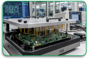
Test and Validate with Prototypes
No amount of simulation replaces a physical prototype. Build, test, and get DFM feedback on your prototype before committing to production quantities. The cost of a prototype respin is always less than the cost of a production line stoppage.
FAQs
What Is the Main Goal of DFM in PCB Design?
The main goal is to ensure that the PCB design can be manufactured consistently, efficiently, and within acceptable cost and quality limits, without requiring special handling, manual intervention, or repeated rework.
When Should DFM Checks Be Performed?
DFM checks should start during the PCB design phase and continue through layout completion, prototype review, and pre-production sign-off. The earlier an issue is found, the cheaper it is to fix.
How Does DFM Reduce PCB Cost?
DFM improves first-pass yield, reduces scrap and rework, shortens production cycle times, and prevents the need for expensive engineering changes after production begins. All of these translate directly into lower unit costs.
Is DFM Only for Large-Scale Production?
No. DFM benefits apply at any volume. Even for a ten-board prototype run, DFM-compliant designs produce more reliable results and make the transition to higher volumes much smoother when the time comes.
Conclusion
DFM is not an optional step, it is what separates designs that build well from designs that cause problems every time they hit the factory floor.
Every trace width decision, every pad size, every component placement choice, and every stack-up call either makes your board easier or harder to manufacture. Getting those decisions right during design costs almost nothing. Getting them wrong during production costs significantly more than anyone budgets for.
PCB Runner supports engineering teams through DFM review, prototype builds, and full production, helping designs move from concept to scalable manufacturing without the painful surprises that come from skipping this step.
“Design it right the first time. DFM is not extra work, it is the work that makes everything else work.”

