
AI data centers are growing faster than the supply chain can keep up, and PCBs are where the whole system is getting stuck. The numbers tell the story clearly. Global AI data center investment crossed $200 billion in 2025 and is accelerating through 2026. Every server rack, every GPU cluster, and every high-speed networking switch in those facilities depend on printed circuit boards. Right now, the PCB Capacity Bottleneck in AI Data Centers is worsening in 2026, as PCB capacity simply cannot keep up with growing industry demand. This is not a minor supply hiccup. It is a structural constraint slowing AI infrastructure deployment worldwide.
PCB Runner works directly in this supply chain. What we are seeing in 2026 is real pressure, longer lead times, tighter material availability, and increasing complexity in what AI hardware actually demands from a PCB. This guide breaks down exactly what is happening and why it matters.
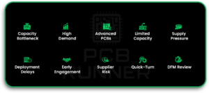
Key Takeaways
- PCB capacity has become a serious bottleneck for AI data center growth in 2026.
- AI data centers need large volumes of advanced PCBs for servers, GPU boards, networking switches, backplanes, and power systems.
- AI server PCBs are more complex than standard boards. They often need high layer counts, HDI structures, controlled impedance, low-loss materials, and better thermal performance.
- Manufacturing capacity for advanced PCBs is limited because only a smaller group of facilities can build these boards reliably.
- Material shortages, longer lead times, and rising demand are increasing pressure on AI hardware supply chains.
- PCB delays can slow server assembly, data center deployment, and customer delivery schedules.
- Companies should engage PCB suppliers early, share forecasts, and qualify more than one capable manufacturing partner.
- Choosing the lowest-cost supplier can create more risk if the supplier cannot meet advanced AI PCB requirements.
- Quick-turn PCB manufacturing helps AI hardware teams prototype faster and support repeated design revisions.
- Designs reviewed for manufacturability before release are more likely to build faster, cost less, and avoid production delays.
The Rapid Growth of AI Data Centers in 2026
Why AI Infrastructure Demand Is Surging
The adoption of large language models, generative AI tools, and autonomous systems has moved from research labs into commercial deployment at a massive scale. Every company running AI inference or training workloads needs dedicated hardware infrastructure. That means more data centers, more servers, and more of everything inside them, including PCBs.
Cloud providers, hyperscalers, and enterprise IT teams are all expanding simultaneously. The result is a steep demand curve showing no signs of flattening.
Role of GPUs, Servers, and High-Speed Electronics
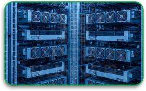
Modern AI workloads run on GPU clusters, often thousands of GPUs networked together inside a single facility. Each GPU board, each server backplane, each networking switch, and each power distribution unit contains multiple printed circuit boards. A single AI server chassis can contain ten or more PCBs of varying complexity. Multiply that across hundreds of thousands of servers being deployed globally, and the scale of PCB demand becomes clear.
Increasing Complexity of AI Hardware Systems
AI servers are not standard computing hardware. They run at higher power densities, generate significantly more heat, and require much faster data transfer between components than conventional servers. This complexity does not just affect the design of the boards, it directly affects how hard they are to manufacture and how few facilities worldwide can actually build them.
Understanding the Role of PCBs in AI Data Centers
How PCBs Power Servers, GPUs, and Networking Equipment
PCBs are the physical platform on which every electronic component in a data center operates. They carry power, route signals, and connect processors, memory, storage, and networking interfaces. Without a functioning PCB, none of the silicon in an AI server does anything.
Importance of High-Speed Signal Transmission
AI workloads move enormous volumes of data between GPUs, between servers, and between nodes in a cluster. PCBs in these systems must support signal speeds of 112 Gbps per lane and above, with tight impedance control, minimal signal loss, and precise layer management. Standard PCB fabrication processes cannot meet these requirements. Specialized materials, tighter tolerances, and advanced stack-ups are mandatory.
Thermal and Power Challenges in AI Hardware
A high-end AI GPU can consume 700 watts or more. Boards carrying these loads must handle extreme thermal stress while maintaining signal integrity. This demands specific copper weights, thermal vias, and materials with higher glass transition temperatures than standard FR-4. These are not commodity PCBs, they are precision-engineered components in their own right.
Why AI Server PCBs Are Different From Traditional PCBs
AI server PCBs are different because they are built for speed, heat, density, and power. A traditional PCB may support basic computing, consumer electronics, or standard industrial equipment. An AI server PCB has to support high-speed GPU communication, dense routing, large power loads, and constant thermal stress.
The difference is not just in the board size or layer count. It is in the performance expectation. AI hardware needs PCBs that can move data quickly without signal loss, carry high current without overheating, and stay stable under continuous load.
Traditional PCBs often use standard FR-4 materials and simpler stack-ups. AI server boards often require advanced laminates, controlled impedance, HDI structures, heavier copper, and tighter manufacturing tolerances. This makes them harder to design, harder to fabricate, and harder to qualify for production.
This is one reason PCB capacity has become such a serious issue. The industry does not only need more boards. It needs more advanced boards that fewer manufacturers can build properly.
Materials Commonly Used in AI Infrastructure PCBs
AI infrastructure PCBs often require materials that can handle high speed, high heat, and low signal loss. Standard FR-4 is still used in many electronics, but it is not always enough for advanced AI servers and networking equipment.
Low-loss laminates are commonly used because they help preserve signal quality at high frequencies. Materials such as Rogers, Megtron 6, and Panasonic Megtron 7 are often selected for demanding AI hardware applications. These materials help reduce signal loss and support faster data transmission.
High-Tg materials are also important. They help the board remain stable at higher operating temperatures. This matters because AI servers generate significant heat during training and inference workloads.
Specialty copper foils and high-performance prepregs may also be required. These materials improve power handling, signal quality, and thermal performance. The challenge is that these materials are not as widely available as standard PCB materials. They also require more careful handling during fabrication.
That is why material availability is now directly tied to AI data center growth. When advanced laminates and specialty copper are delayed, the boards are delayed too.
Why HDI Manufacturing Matters for AI Hardware
High Density Interconnect PCB technology is becoming essential for AI hardware because AI boards need more routing in less space. GPUs, memory modules, power systems, and high-speed interfaces are packed tightly together. Standard via structures are often not enough to support this level of density.
HDI manufacturing uses microvias, blind vias, and buried vias to create shorter and more efficient signal paths. This helps designers fit more connections into a smaller board area while also improving electrical performance.
For AI hardware, this matters because signal speed and layout density are both critical. Long or poorly controlled signal paths can create performance issues. HDI helps reduce these risks by allowing more direct routing between important components.
HDI also supports smaller component packages and more complex board designs. As AI servers continue to become more powerful, HDI will become less of an advanced option and more of a standard requirement.
The challenge is that HDI manufacturing requires laser drilling, tight registration control, advanced inspection, and strong process experience. Not every PCB manufacturer can build HDI boards reliably, especially at the layer counts and tolerances required for AI infrastructure.
Why PCB Capacity Is Becoming a Bottleneck
Limited Manufacturing Capacity for Advanced PCBs
The global PCB industry has significant total capacity, but most of it is built for standard consumer and industrial electronics. The capacity for high-layer-count, controlled-impedance, high-frequency boards that AI hardware requires is concentrated in a small number of facilities. Those facilities are now fully booked.
Rising Demand for Multilayer and High-Density Boards
AI server boards commonly require 16 to 32 layers or more. High-Density Interconnect PCB technology, with microvias, blind vias, and buried vias, is increasingly required as component density increases. Producing these boards requires specialized equipment and process control that most mid-tier PCB manufacturers simply do not have.
Supply Chain Constraints and Material Shortages
The raw materials for advanced PCBs, low-loss laminates, high-Tg prepregs, and specialty copper foils, are supplied by a limited number of suppliers. When demand surges suddenly, as it has with AI, material lead times extend and allocation windows tighten. This feeds directly into longer board lead times downstream.
Key Factors Driving PCB Supply Constraints
Complexity of High-Layer Count PCBs
Each additional layer in a multilayer PCB adds lamination cycles, registration requirements, and inspection complexity. A 24-layer board is not just twice as hard to build as a 12-layer board, it is exponentially more demanding in terms of process control, equipment precision, and yield management.
Need for Advanced Materials and Precision Manufacturing
AI PCBs require laminates with dielectric constants below 3.5 and loss tangents below 0.005, specifications that only high-frequency materials like Rogers, Megtron 6, or Panasonic Megtron 7 can meet. These materials are harder to process, more expensive, and available from fewer sources than standard FR-4.
Increased Lead Times Across Global Supply Chains
Before the AI infrastructure surge, lead times for complex multilayer boards ran 4 to 6 weeks. In 2025 and into 2026, lead times for advanced AI server boards have extended to 12 to 20 weeks at many facilities, and, in some cases, longer for specific, material-dependent designs.
Impact of PCB Shortages on AI Data Center Growth
Delays in Server and Hardware Deployment
When PCBs are delayed, server assembly stops. When server assembly stops, data center commissioning is pushed back. For companies under commercial pressure to deliver AI services on schedule, these delays have direct revenue consequences.
Rising Costs for AI Infrastructure
Constrained supply pushes prices up. PCB fabrication processes for advanced boards have seen cost increases of 20 to 40 percent in some categories since 2024. These cost increases flow through to server OEMs, system integrators, and ultimately to end customers building AI infrastructure.
Pressure on OEMs and System Integrators
Original equipment manufacturers building AI servers are caught between GPU suppliers, PCB suppliers, and customers, all with competing schedules. The PCB is often the longest lead-time item in the bill of materials, making it the critical path in delivery schedules.
Challenges Faced by PCB Manufacturers
Scaling Production Without Compromising Quality
Adding capacity for advanced PCBs is not as simple as buying more machines. Advanced boards require process calibration, operator training, and yield validation, all of which take months to establish. Scaling too fast risks quality failures that damage customer relationships and increase scrap costs.
Investment Requirements for Advanced Equipment
Laser-drill equipment for microvia fabrication, advanced direct-imaging systems, and automated optical inspection tools for fine-feature boards cost millions of dollars per unit. For most PCB manufacturers, this level of capital investment requires long-term volume commitments before it can be justified.
Skilled Workforce and Technical Limitations
Advanced PCB fabrication requires engineers and technicians who understand controlled impedance, via reliability, signal integrity, and precision lamination. This talent is scarce globally and takes years to develop. The workforce constraint is as real as the equipment constraint.
How AI Hardware Requirements Are Changing PCB Design
Shift Toward High-Density Interconnect (HDI) Designs
High Density Interconnect PCB designs use microvias, drilled by laser rather than mechanical drill, to achieve much higher routing density than standard through-hole via technology allows. HDI is now the baseline requirement for many AI server and networking applications, not an advanced option.
| Feature | Standard PCB | HDI PCB |
| Via type | Mechanical through-hole | Laser microvias, blind/buried vias |
| Minimum via diameter | 0.2 mm | 0.075 mm or smaller |
| Layer count typical | 4–8 layers | 8–32+ layers |
| Signal speed support | Up to ~10 Gbps | 56 Gbps, 112 Gbps, and beyond |
| Manufacturing complexity | Standard | High to very high |
Increased Layer Counts and Complex Stack-Ups
AI networking and compute boards increasingly require 20 to 32 layers, with controlled impedance on multiple layers simultaneously. Stack-up design must be coordinated with the fabricator from the very beginning of the design process, not finalized and then handed over.
Higher Power Density and Thermal Design Needs
Boards carrying 400W to 700W components need heavy copper, 2 oz to 4 oz, on power planes, thermal relief structures under high-dissipation packages, and materials that maintain mechanical integrity at sustained elevated temperatures. These requirements immediately eliminate most standard fabricators from consideration.
Strategies to Overcome PCB Capacity Constraints
Expanding Manufacturing Capabilities
Leading PCB manufacturers are investing in new lines specifically for high-layer-count and HDI production. This expansion is happening simultaneously in Asia, North America, and Europe, but the timelines for new capacity to come online range from 18 to 36 months from the investment decision to qualified production.
Diversifying Supply Chains
Companies that relied on a single PCB supplier for advanced boards have discovered the fragility of that approach. Qualifying two or three capable manufacturers for critical boards, even at slightly higher unit cost, provides resilience that single-source dependency cannot.
Adopting Advanced PCB Fabrication Processes
Semi-additive processes, advanced laser direct imaging, and automated inline inspection are enabling higher yields on complex boards at some leading manufacturers. These process improvements increase throughput on existing lines without requiring entirely new facilities.
Role of Quick-Turn PCB Manufacturing in Addressing Demand
Faster Prototyping for AI Hardware Development
AI hardware design cycles are compressing. Teams that would previously spend three months on prototype iterations are now expected to complete the same work in three weeks. Quick-turn fabrication capability, boards in five to ten days, is essential for maintaining this pace.
Reducing Time-to-Market for New Systems
In a competitive AI hardware market, being first to production matters enormously. Quick-turn capability at the prototype stage accelerates every downstream phase, validation, regulatory testing, pilot production, and full ramp.
Supporting Iterative Design Cycles
Complex AI boards rarely go from prototype to production without revisions. Quick-turn manufacturing supports the multiple design-test-revise cycles needed to validate a high-complexity board before committing to production tooling.
What Businesses Should Consider When Planning PCB Supply
Early Supplier Engagement and Forecasting
Share your 12-month production forecast with your PCB manufacturer as early as possible. Manufacturers allocate capacity to customers with committed forecasts first. Companies that show up with urgent orders and no prior engagement consistently end up at the back of the queue.
Choosing the Right Manufacturing Partner
Not every manufacturer can build AI-class PCBs. Before committing to a supplier, confirm their layer count capability, minimum via sizes, controlled impedance experience, and the specific materials they can process. Ask for evidence, not just claims.
Balancing Cost, Speed, and Quality
In a constrained supply environment, chasing the lowest price on advanced boards is a false economy. A board that fails qualification costs far more in schedule delay than the price premium of a capable, quality-focused manufacturer.
Future Outlook: Will PCB Capacity Catch Up With AI Demand?
Industry Investments and Expansion Plans
Major PCB manufacturers in Taiwan, South Korea, Japan, and increasingly in the United States and Europe are committing significant capital to advanced fabrication capacity. These investments are real and substantial, but they will not produce qualified production output until 2027 and beyond for most projects.
Emerging Technologies in PCB Manufacturing
Embedded component technology, 3D-printed PCBs for prototyping, and additive copper processes are all advancing. These technologies will not replace conventional subtractive fabrication in the near term. Still, they will expand the options available for specific applications and reduce pressure on conventional capacity for some board types.
Long-Term Supply Chain Stabilization
The current imbalance between AI hardware demand and PCB manufacturing capacity is not permanent. Supply will catch up, it always does. But the companies that manage through the constraint period successfully will have significant advantages in cost, schedule, and supplier relationships on the other side.
Common Mistakes Companies Make in High-Demand Environments
Underestimating Lead Times
Planning a product launch around six-week PCB lead times when the actual market lead time is sixteen weeks guarantees a missed schedule. Always get current lead-time information from your actual supplier—not industry averages from six months ago.
Relying on a Single Supplier
A single-source dependency for a critical, long-lead component is a risk that is very difficult to justify in 2026. Qualification of a backup supplier takes time, start now, before you need it.
Ignoring Design Optimization for Manufacturability
A design that pushes beyond your manufacturer’s process capability will generate engineering queries, require design revisions, and add weeks to your schedule. Designs reviewed for manufacturability before release build faster, yield better, and cost less. This is always true, but in a constrained supply environment, it is especially consequential.
FAQs
Why Are PCBs Critical for AI Data Centers?
Every server, GPU board, networking switch, and power system in an AI data center is built on printed circuit boards. PCBs power, route signals, and connect all the components that enable AI computation. Without them, AI hardware does not function.
What Type of PCBs Are Used in AI Servers?
AI servers use high-layer-count multilayer boards, typically 16 to 32 layers, with controlled impedance, HDI microvia structures, low-loss laminates, and heavy copper on power planes. These are among the most technically demanding PCBs produced commercially.
How Long Are Current PCB Lead Times?
For standard FR-4 boards, lead times remain relatively short at three to five weeks. For advanced AI-class boards with high layer counts, HDI features, and specialty materials, lead times in 2026 are running twelve to twenty weeks at many qualified manufacturers, and longer for designs with specific material requirements.
How Can Companies Avoid PCB Supply Delays?
The most effective steps are: engage your PCB manufacturer early with volume forecasts, qualify your design for manufacturability before release, build relationships with two or more capable suppliers, and never plan production schedules around best-case lead time assumptions.
Conclusion
PCB capacity is not a background logistics issue, it is one of the defining constraints on how fast AI infrastructure can actually be built in 2026.
The demand is real, the complexity is increasing, and the manufacturing base for advanced boards is not expanding fast enough to keep pace with AI hardware deployment. Companies that understand this constraint and plan around it will deliver on schedule. Those who treat PCB supply as a commodity procurement problem will face the delays that are already becoming the norm.
PCB Runner supports hardware teams building AI infrastructure, from design review through prototype and into production, with the technical capability and honest lead-time guidance that complex programs require.

