When you send your design for PCB fabrication in Europe, there are many hidden steps that make sure your board comes out strong and reliable. One of these is known as copper thieving. In this article, you will find out the meaning of copper thieving and how it works, the reasons why it’s used, and the reasons it is essential to the printed circuit board (PCB) project.
This blog will help you understand why copper thieving is crucial and how it impacts the PCBs you use during fabrication as well as manufacturing.
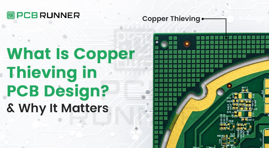
What Is Copper Thieving in PCB Design?
Copper thieving can be described as a pcb design method used on circuit boards to control how much copper is used across the board. When excessive copper characterises a board in one region but not enough in the other, it can cause problems when manufacturing.
Imagine copper thieving as making small patches of copper in spaces that are empty. These patches aren’t an electrical connection. They help place the plate on the board and also help ensure that the etching is evenly distributed in the factory. This improves overall quality and decreases the chance of imperfections.
Thieving copper aims to make a uniform copper pattern. Manufacturers employ it to prevent uneven plating and stresses in the boards. This is particularly important for manufacturing PCBs in Europe and worldwide boards that require a high level of precision.
Why Is Copper Thieving Important?
Copper thieving plays a crucial function in ensuring that your PCB is constructed in the same way as it was designed. Here are the primary factors that matter:
Better Plating During Manufacturing
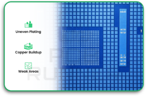
When a board is coated with copper, it is deposited on the surface. If one region is saturated with copper, while the other has tiny amounts, the plating bath may not saturate the copper in a uniform manner. This could cause:
- Uneven plating may lead to areas that are under-plated or over-plated.
- Extra-thick copper in other areas
- Defects or weak spots
Copper thieving assists in balancing this process. It provides a more uniform layer for plating to run effortlessly.
Reduce Warpage and Stress
Uneven distribution of copper can cause the board to swell as it is exposed to chemicals and heat. Warped boards are more challenging to put together and could be damaged in the course of use. Copper thieving reduces stress and warpage, making boards more stable and reliable..
Improve Yield and Reduce Waste
Boards that are etched and appropriately plated are more likely to get through quality inspections. This means that fewer boards are being discarded. Businesses that utilise PCB fabrication assembly. This reduces the cost and increases the speed and efficiency.
Improve Thermal Balance
Copper is an excellent conductor of heat. Regions that have a high concentration of copper will get hotter than areas that have less copper. Unbalanced heat flow could create stress.
When you integrate copper thieving with thermal management on PCBs, this helps to maintain the balance of heat flow throughout the board. This helps improve performance and a longer lifespan.
Copper thieving is maily tied to copper density (copper balance) rules, where PCB manufacturers do prefer a more uniform copper distribution across each layer and even across the full panel/array, especially for larger pcb/panel dimensions because extreme differences (example: one area having very high copper coverage while another is mostly empty laminate) can create issues like warpage. For e.g: During the CAM/DFM stage, PCB Runner team may propose the panel along with the add on copper thieving patterns in open areas of the board or panel rails to stabilize plating, reduce warpage risk, and improve overall manufacturing yield.
How Does Copper Thieving Work?
The most common method of copper thieving is by placing patterns of tiny copper shapes inside blank areas on the board. These designs aren’t connected to any other component or signal. They’re designed to help balance the distribution of copper.
Common Patterns
The most common patterns are:
- Small dots
- Square patches
- Grid patterns
The pattern you choose is dependent on the design of the board as well as the location where copper is required.
Where Thieving Is Placed
Thieving is usually categorised as:
- In large empty spaces
- Near areas that have a heavy trace of copper
- Between pads and in holes
The designers of boards place these shapes in a strategic manner. They need to ensure that copper thieving doesn’t interfere with the electrical performance.
Copper Thieving vs Copper Pour Techniques
Copper thieving does not serve an electrical function. It only supports manufacturing. Here’s a simple comparison:
| Feature | Copper Thieving | Copper Pour Techniques |
| Purpose | Balance copper for manufacturing | Provide electrical plane/function |
| Connection | Not connected to nets | Connected to nets (e.g., ground) |
| Effect | Helps plating and etching | Supports signal/power distribution |
Both are useful, but they serve very different roles. When working with PCB fabrication in Europe partners, it is important to understand these differences.
What Is Copper Pour?
Copper pour refers to the process whereby large portions of a board are filled with copper and utilised to perform electrical functions. Examples:
- Ground planes
- Power planes
- Shielding zones
These areas are able to carry current or serve as reference points.
How Thieving Is Different
Copper thieving does not serve an electrical purpose. It is only used to support manufacturing. Here’s a fundamental analysis:
Both are valuable, but they have very different functions. In working together with PCB manufacturing Europe partners It is crucial to know the differences.
When Is Copper Thieving Most Helpful?
Copper thieving is extremely useful in boards with:
- Large open spaces
- High-density routing
- Uneven copper distribution
- Complex multilayer structures
These are typical of boards manufactured using Pcb fabrication assembly services in Europe and in the UK.
High-Density Boards
Boards that have a lot of fine lines and very little space can benefit from tiny areas of thieving in order to ensure uniform plating.
Boards With Large Empty Zones
The large empty spaces with no copper could cause an uneven chemical reaction. Adding thieving patterns in empty zones balances copper distribution and ensures uniform plating and etching.
Multilayer Boards
Multilayers are much more intricate. Each layer could have diverse layouts of copper. Thieving can help maintain the balance of the layer during the process of plating or lamination.
Best Practices for Copper Thieving
When you design copper thieving into your PCB, adhere to these guidelines:
1. Keep It Out of Signal Areas
Thieving should not affect the electrical signals. Avoid it near sensitive circuits.
2. Maintain Adequate Clearances
Be sure that the copper that is stolen is not in proximity to any components or traces. This prevents the possibility of accidental shorts.
3. Use Small, Even Patterns
Smaller patterns with evenly spaced spacing are simpler to make and are less likely to impact performance.
4. Check With Your Manufacturer
Always consult your PCB fabrication partner for specific guidelines. Certain manufacturers want to limit the places where thieving occurs.
If you are working with PCB runners as well as similar fabricators, the communication is clear and ensures that thieving is done in a safe manner without impacting the design.
Common Mistakes With Copper Thieving
Although copper thieving is beneficial, there are some mistakes that designers often make:
- thieving occurring too close to trace
- By using large copper areas that behave like pours that aren’t intended to be
- Intentionally omitting to prevent thieving from the RF or analogue areas that are sensitive
- Unverified Design rule check (DRC)
Avoid these errors to ensure your design is secure and efficient.
Does Copper Thieving Affect Electrical Performance?
This is a problem that’s common. The answer is simple: Not if it is done properly.
Thieving is carried out in unused areas. It’s not part of any electrical network. If it is located at a safe distance and abides by specifications, it should not affect electrical behaviour.
But, if the copper is connected or too close without intention, it may:
- Can introduce parasitic capacitance or unintended coupling.
- The effect of high-speed signals
- Create paths that aren’t intended to be
Always verify your design using tools such as DRC before submitting it to the PCB’s fabrication in Europe and assembly.
How Do Manufacturers Use Copper Thieving?
Manufacturers typically add thieving regions where they observe huge copper imbalances. It can occur during:
- Electroplating
- Etching
- Soldermask application
Manufacturers may add copper thieving themselves if it is not included in the design. This is why it’s crucial to know how they handle it.
Factories across Europe and all over the world employ thieving for:
- Increase yield
- Reduce defects
- Lower production costs
- Increase the reliability of the board
Also Read:
Copper Thieving and Thermal Management in PCBs
Good thermal management in PCBs is vital to the board’s durability. Copper conducts heat efficiently. Uneven copper can cause cool or hot spots.
Copper thieving assists in spreading warmth more uniformly. It doesn’t replace the thermal through-pipes or heat sinks, but it does help with heat distribution in areas where no spaces are present.
The balance of copper can also help in the event that your board experiences heat stress during manufacturing and usage.
FAQs
1. What is copper thieving, and what does it have to do with the PCB manufacturing process in Europe?
Copper thieving is used to ensure that the balance of copper on a board is achieved prior to manufacturing. When it comes to the PCB manufacturing industry in Europe, it can help prevent plating flaws and provide better quality production.
2. Does copper thieving influence the fabrication of PCBs’ quality?
A: Yes. If properly used, copper thieving can improve the fabrication of PCBs by decreasing warpage, preventing uneven plating and reducing production defects.
3. How does copper thieving differ from copper pour techniques?
A: Copper thieving can be employed only to balance manufacturing. Copper pour techniques are employed to create electrical functional areas such as ground planes. Thieving doesn’t carry signals.
4. Does copper thieving help enhance the thermal management in PCBs?
A: Yes. Copper thieving helps distribute heat more evenly. This helps improve thermal management on PCBs, although it’s not the main cooling option.
Conclusion
Copper thieving is one of the design tricks which can have a significant effect on how your PCB will turn out. It assists in balancing copper, enhances plating and etching, and ensures that there are no costly issues in the PCB fabrication in Europe, as well as PCB fabrication assembly.
Understanding the thieving of copper can help you design more intelligent boards. This also lets you communicate with companies like PCB Runner. This will result in stronger and more durable PCBs that are printed on.

