


Objective
Help engineers and procurement teams understand where PCB Assembly Failures actually originate, so they can catch problems at the design and quoting stage rather than paying for them after a batch has already failed.
Key Takeaways
- Most PCB Assembly Failures start before assembly ever begins, often at the design stage
- Solder defects, component placement errors, and thermal stress account for the majority of field failures
- A proper DFM review catches the bulk of these issues before manufacturing starts
- Working with an experienced PCB manufacturer reduces rework far more than chasing the cheapest quote
- Testing and inspection at multiple stages, not just at the end, is what actually prevents failures reaching the customer
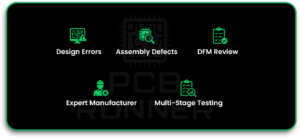
A customer once brought us a batch of 500 boards that had passed every visual check and still failed in the field within weeks. The solder joints looked fine under a loupe. The problem was hiding underneath a QFN package, invisible without an X-ray. That’s the thing about PCB Assembly Failures: the ones that hurt the most are rarely the ones you can see.
Most failures don’t happen because someone was careless on the line. They happen because a decision made weeks earlier, at the design stage or the material selection stage, quietly sets the board up to fail. By the time it shows up as a dead unit in the field, tracing it back costs far more than catching it would have.
This is the part of the job that separates a PCB manufacturer who just populates boards from one who actually protects your product.
Most PCB failures start before the board ever hits the line, usually at design or material selection. Solder defects, placement shifts, and thermal stress account for most of them, and nearly all are catchable with a proper DFM review. The earlier a failure is caught, the cheaper it is to fix. Field failures cost the most by far.
What Are PCB Assembly Failures
A PCB assembly failure is any defect that stops a board from performing as designed, whether that shows up immediately on the test bench or six months later in a customer’s product.
Some failures are obvious: a bridged solder joint, a missing component, a board that won’t power on. Others are subtle. A cracked solder ball under a BGA package can pass initial testing and still fail after a few thermal cycles.
The distinction matters. Catching an obvious failure costs you a rework cycle. Catching a subtle one after shipment costs you a recall, a warranty claim, and a customer who won’t order again.
Common Causes of PCB Assembly Mistakes
Solder defects. Bridging, tombstoning, insufficient wetting, and voiding account for a large share of assembly problems. Most trace back to paste volume, stencil design, or a reflow profile that wasn’t matched to the board’s thermal mass.
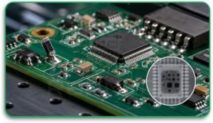
Component placement errors. Fine-pitch parts, like 0.25mm pitch ICs, need tight placement accuracy. A shift of even a fraction of a millimetre can cause an open connection that won’t show up until the board is under load.
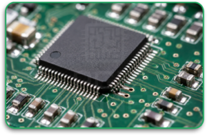
Thermal stress during reflow. Running one standard reflow profile across every job is a common shortcut. Boards with mixed component types, or a metal core substrate, need a profile built around their specific thermal mass, not a generic setting.
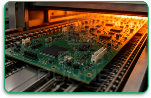
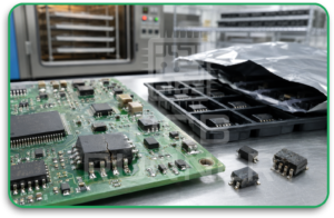
Moisture-related defects. Components left out of moisture barrier bags too long before reflow can develop “popcorning,” where trapped moisture flashes to steam and cracks the package during soldering. This one’s entirely preventable with proper handling and baking.
Contamination. Flux residue, dust, or handling oils on the board surface interfere with solder wetting and can cause long-term corrosion under the coating.
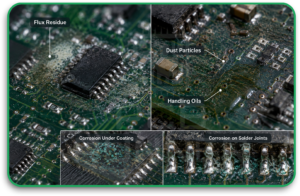
These are the everyday PCB Assembly mistakes that a controlled process is built to catch, not eliminate through luck.
How the PCB Design Process Contributes to Failures
A lot of assembly failures are actually design failures wearing an assembly costume.
Tight component spacing that looked fine in the CAD tool can leave no room for solder paste to flow properly during reflow. Pads sized without considering the actual reflow profile lead to tombstoning, where one end of a component lifts off the pad.
Poor thermal relief on ground planes causes uneven heating during soldering, so some joints reflow properly while others stay cold. This is why we review every stack-up before the layout even starts. Our own PCB design process builds Design for Assembly and Design for Manufacturability into the layout stage, rather than treating them as an afterthought once the board reaches the assembly line.
A board designed without assembly in mind will always cost more to build, however good the schematic looks on paper.
How PCB Runner Prevents PCB Assembly Failures
We review every CAM file before manufacturing starts, at no charge. That single step catches a large share of the issues that would otherwise show up as PCB failure reports months later.
Our inspection process runs at multiple stages, not just at the end of the line. We use AOI to catch placement and solder defects visually, X-ray for hidden joints under BGA and QFN packages, and In-Circuit Testing to confirm the board actually functions electrically.
We also test our solder profiles against the specific board, rather than running a fixed setting across every job. A rigid FR-4 board and a metal-core LED board don’t heat the same way, so they shouldn’t be soldered the same way either.
What to Look for in a PCB Manufacturer
Not every shop treats failure prevention the same way. A few things worth checking before committing a project:
- Free DFM and CAM review. If a manufacturer charges to review your files before quoting, that’s a sign they’re not looking closely.
- In-house inspection capability. AOI alone isn’t enough for hidden joints. Ask whether X-ray and ICT are available on-site.
- Traceability. A manufacturer who can trace a batch back to specific components and reflow settings can actually diagnose a failure instead of guessing.
- No minimum order quantity. Shops with high MOQs push you toward larger, riskier first runs instead of letting you validate a small batch first.
- IPC compliance. Look for assembly performed to IPC-A-610 standards, with fabrication meeting IPC 6011 and IPC 6012.
Cost of Ignoring PCB Failures
| Stage Failure Is Caught | Typical Cost Impact |
| Design review (before layout finalised) | Lowest, usually just design time |
| DFM/CAM review (before manufacturing) | Low, rework limited to files |
| In-process inspection (AOI, X-ray, ICT) | Moderate, scrap or rework a batch |
| Post-shipment field failure | Highest, includes recalls, warranty, and lost trust |
The pattern is consistent across every project we’ve handled: the earlier a PCB Assembly Failure is caught, the cheaper it is to fix. A failure caught on the test bench costs a fraction of one caught in a customer’s product.
Conclusion
Most PCB Assembly Failures are preventable, and the fix usually starts earlier than people expect, at the design and file review stage, not on the line.
If you want your next board reviewed before it goes anywhere near production, contact PCB Runner for a free DFM and CAM review. Call +44 203 2397011 or email sales@pcbrunner.com.
FAQs
How do I know if my board failed because of design or because of assembly?
Start with where the defect sits. Cold joints, bridging, and placement shifts usually point to the assembly process. Thermal relief issues, insufficient spacing, or pad sizing problems usually trace back to the design itself. A good manufacturer will tell you honestly which it is, not just blame the other side.
Can you catch hidden solder defects under BGA packages?
Yes. Visual inspection can’t see under a ball grid array, so we use X-ray specifically for these joints, alongside AOI for everything visible on the surface.
What’s the fastest way to reduce PCB Assembly Failures on a new product?
Get a DFM review done before you commit to a full production run. We do this free of charge, and it catches most of the issues that would otherwise surface after the boards are built.
Do you charge for reviewing our design files before quoting?
No. We review CAM files and BOMs before quoting on every project, regardless of order size.
What happens if a batch fails after we’ve already received it?
Contact us with the specific defect and batch details. Because we track components and process settings per job, we can usually trace the cause and correct it on the next run, rather than guessing.



