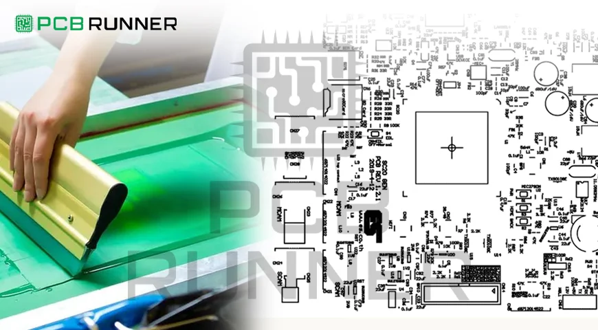
When you look at a custom-printed circuit board, you’ll notice small white markings on its surface. These markings, known as the silkscreen layer, provide essential information about the board’s components, reference designators, part numbers, and symbols. A silkscreen PCB helps engineers, manufacturers, and technicians correctly assemble and troubleshoot the board.
Let’s explore what else a silkscreened PCB entails, how it is manufactured and its significance in pc board assembly. In this article, we will try to cover the silkscreen printing methods, their pros, and how to get rid of or maintain them if need be.
When designing multilayer printed circuit boards or dealing with PCB sales representatives, knowledge of the silkscreen industrial process would aid in enhancing the quality and efficiency of PCB production.
What is a Silkscreen PCB?
As the name suggests, a silkscreen PCB is a type of printed circuit board where a silkscreen layer has been applied. This layer, usually composed of a plastic ink cover, is printed on the board to give names, identifiers of components, and even a brand name if there is the need to do so.
You will find that most production companies will have this layer printed in white ink, while some opt for yellow, black, red or any other colour of their choosing based on custom design options.
The silkscreen layer clearly has great significance as it enables:
- Shows company logos and warning signage.
- Assists in troubleshooting and repairs.
- Enhances the readability of custom printed circuit board designs.
In multilayer printed circuit boards, the silkscreen layer is typically limited to the top and bottom layers for easier assembly and inspection in the printed circuit board (PCB) fabrication processes.
The Process of Making a Silkscreen PCB
To create a silkscreen PCB, there are several varied steps to guarantee that the end board will be accurate, clear, and a good as long-lasting.
1. Getting the PCB Ready for Printing Design
The PCB designer prepares the files on a CAD program, creating the silkscreen layer where all the text, symbols and markings will be placed in accordance with the PCB layout, which is sent to the PC board assembly manufacturer for fabrication.
2. Selecting the Printing Method
Silkscreen printing can be added directly onto the PCB with three methods.
1. Manual Screen Printing:
- Uses a stencil or mesh screen to apply epoxy ink to the board.
- Ideal for small-quantity production.
- Requires both drying and curing to set the ink.
2. Liquid Photo Imaging (LPI):
- Imprints light-sensitive ink and exposes it using a mask with a UV light.
- Gives out higher resolution markings than manual printing.
- Used on most sophisticated, high-density boards.
3. Direct Legend Printing (DLP):
- An inkjet printer applies UV-curable ink directly to a printed circuit board.
- No requirement for either masks or stencils.
- Best suited for multilayer printed circuit boards with high accuracy.
3. Inspection of the PCB Quality and Ink Curing
Following the printing, the board is inspected for proper alignment, fading, or smudging before moving on to pc board assembly. Next, the ink is cured utilizing heat or UV light during the inspection stage.
Problems Relating to PCB Silkscreen
Despite the precision of silkscreen PCBs printing, some common problems may still arise:
1. Misalignment
- If the silkscreen layer is misaligned, component identifiers may overlap and become unreadable.
- High precision alignment techniques are used in order to circumvent this problem.
2. Smudged Ink and Fading Text
- Over time, due to poor-quality ink or improper curing, the text may fade.
- Durability can be improved by using UV curable or epoxy-based inks.
3. Overcrowded Symbols and Letters
- The text or symbol set may become cluttered if there is too much component density.
- Designers should optimize spacing to enhance readability and avoid clutter.
How to Remove Silkscreen from PCB?
A silkscreen can be removed for a PCB. Whether it may be used to modify a board or it may be used to clean an area for rework to correct a labelling mistake. Here’s how you do it:
1. Wash Off with Isopropyl Alcohol (IPA)
- Take a cotton swab and put IPA (99% Alcohol) on it.
- Carefully scrub under the silkscreen markings.
- This approach aids in the light removal of ink without causing damage to the PCB.
2. Acetone or Nail Polish Remover
- Get a cloth and pour in a bit of acetone.
- Slowly wipe to aid in the dissolution of the ink.
- However, bear in mind that excessive amounts of acetone can damage PCB coatings.
3. Fine Sandpaper or Scraping
- For tougher inks, some ultra-fine sandpaper (1000+ grit) can be used.
- Gently rub in the area until the ink is entirely removed.
- Use with caution, as too much pressure can lead to damage to the copper traces.
The Importance of Silkscreen for PCB Manufacturing
Silkscreen is vital in PC board assembly as it helps engineers and technicians to:
- Locate components in a few seconds during assembly.
- Mark polarity and orientation to prevent assembly mistakes.
- Use reference designators for faulty board troubleshooting.
- Increase productivity in the sales and production of high-volume PCBs.
- The presence of silkscreen in multilayer printed circuit boards helps in reducing misplacement and speeding up the assembly process.
Finding The Best Silkscreen For Your PCB
When working with a PCB circuit board manufacturer, keep these points in mind when choosing a silkscreen method:
1. Production Volume
Low volume production: Manual screen printing
Mid volume: Liquid photo imaging (LPI)
High volume: Direct legend printing (DLP)
2. Complexity of PCB
Simple designs: No need beyond manual screen printing.
High-density PCBs: DLP or LPI gives better resolutions.
3. Financial Limitations
- DLP is more expensive but gives the most accuracy.
- Manual screen printing is less expensive, but accuracy is compromised.
Best Practices for Designing a Silkscreen PCB
When designing a silkscreen PCB to increase its readability and usability:
- Use regular typeface (Scrip, stylized fonts and complex fonts should not be used).
- Make sure that the text is at least 0.5mm in height for it to be legible.
- Do not place silkscreen above pads (these are helpful in case soldering is required).
- Use different colours to enhance visibility.
- Confirm that everything is in place before leaving the design stages.
Emerging Developments in PCB Silkscreen Technologies
As we move forward with advances in PCB fabrication, the following improvements are being made in printing silkscreen PCBs:
- Nano-Ink for increased durability and precision.
- AI-Assisted Text Placement for better readable layouts.
- Environmentally friendly inks.
- Smart labels for easy tracking using QR codes and RFID tags.
Final Thoughts
Even though a silkscreen PCB forms a very tiny part of a custom printed circuit board, its functionality is significant regarding assembly, troubleshooting, and design. Be it a self-designed or with a PCB board manufacturer, knowledge of how a PCB silkscreen is made helps improve efficiency and reduce issues.
For etched silkscreens or top-grade PCBs, just reach out to us at PCB Runners, and we will gladly assist you. Our team is ready to take your call for quality pc board assembly and printed multilayer circuit board fabrication services.
FAQs
1. What is a silkscreen PCB?
In comparison to other PCBs, silkscreen PCBs are easier to assemble and troubleshoot because of the text, symbols, and markings that are printed on it.
2. How is a PCB silkscreen made?
A silkscreen PCB can be made through screen printing as well as liquid photo imaging (LPI) or direct legend printing (DLP).
3. How do you remove silkscreen from a PCB?
You can make use of isopropyl alcohol, acetone, or a fine piece of sandpaper to eliminate unwanted silkscreen marking on a PCB.
4. Why is silkscreen crucial in PCB manufacturing?
Silkscreen makes it possible to identify components on a PCB and prevents errors during assembly and repair. Therefore, it increases efficiency.
5. What is the best silkscreen printing method?
For PCBs, silkscreen printing that uses direct legend printing (DLP) makes the deepest impressions on the surface and has excellent longevity.

