The constant evolution of telecommunication systems has extended to mobile networks, the Internet, and even advanced security systems. At its core, a custom printed circuit board (PCB) is developed to underpin the technology, thus forming the backbone of robust, seamless communication.
This blog will discuss the crucial materials and practices involved in telecommunication PCB manufacturing and how technological innovations have made it possible to have smaller, more powerful, and incredibly durable circuit boards.
Telecommunications Custom Printed Circuit Boards Importance
Telecommunication devices are subjected to so many conditions that their environment is often described as hostile. From wireless networks to satellite communication to broadband equipment, the PCBs must always be dependable and durable.
Some of the main functions of PCBs in telecommunication applications include but are not limited to:
- Powering the base stations, network antennas, and servers.
- Transmission and the reception of signals.
- Processing large amounts of data in a short term.
- Because PCBs are sensitive, great care must be taken to ensure their resistance to high frequencies, extreme temperatures, and environmental stress.
Expert Insight
To meet the increasing pressure for improved efficiency with electronic devices, the evolution of materials PCB manufacturing is changing rapidly. The industry standard material FR4 is being supplemented, and in some cases even replaced, by advanced materials like polyimide and ceramic. These materials are able to withstand the high-performance needs of modern applications because of their superior thermal management, flexibility, and durability.
Various industries, such as high-performance computing and telecommunications, have now started to depend on these materials to ensure reliable performance at ever-increasing levels of efficiency and speed requirements.
The materials that define the PCBs used in telecommunication devices require careful selection to achieve performance and durability.
FR4 (Flame Retardant 4)
This material probably takes first place in the world of PCB materials. The advantages of FR4 include:
- Adequate structural integrity.
- Ability to sustain high temperatures.
- Affordability.
- FR4 comes short when used for high-frequency applications due to its limited electrical properties.
Rogers Material
Telecommunication systems that require high signal transmission need advanced materials that have high-frequency laminates, Rogers material offers exactly that. These laminates provide:
- Outstanding dielectric characteristics.
- Appropriate levels of signal attenuation.
- Enhanced thermal management.
Metal-Core PCBs (MCPCBs)
MCPCBs are perfect for applications needing exceptional heat dissipation as they incorporate a metal core (generally aluminum) which helps with the thermal management of the process.
Flexible and Rigid-Flex Materials
Due to their:
- Space savings,
- Ability to bend and fit complex designs,
- Flexible and rigid-flex PCBs are becoming popular in compact telecommunication equipment.
- Techniques in Telecommunication PCB Manufacturing
Manufacturers take precise measures to ensure reliability and efficiency while building PCBs for telecommunication; these include:
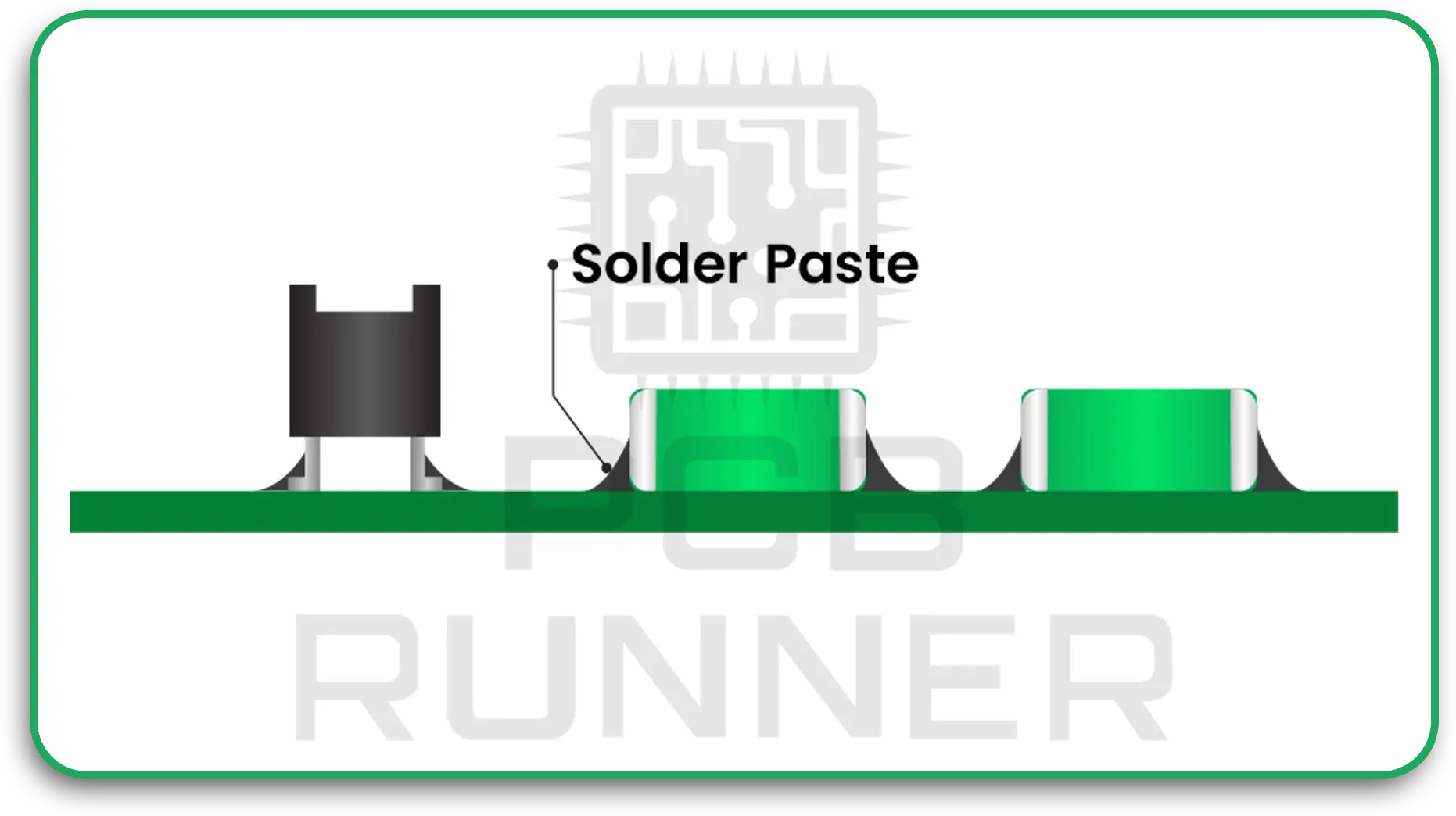
Surface Mount Technology (SMT)
With SMT, components can be mounted directly on the surface of the PCB, allowing for smaller, more compact designs.
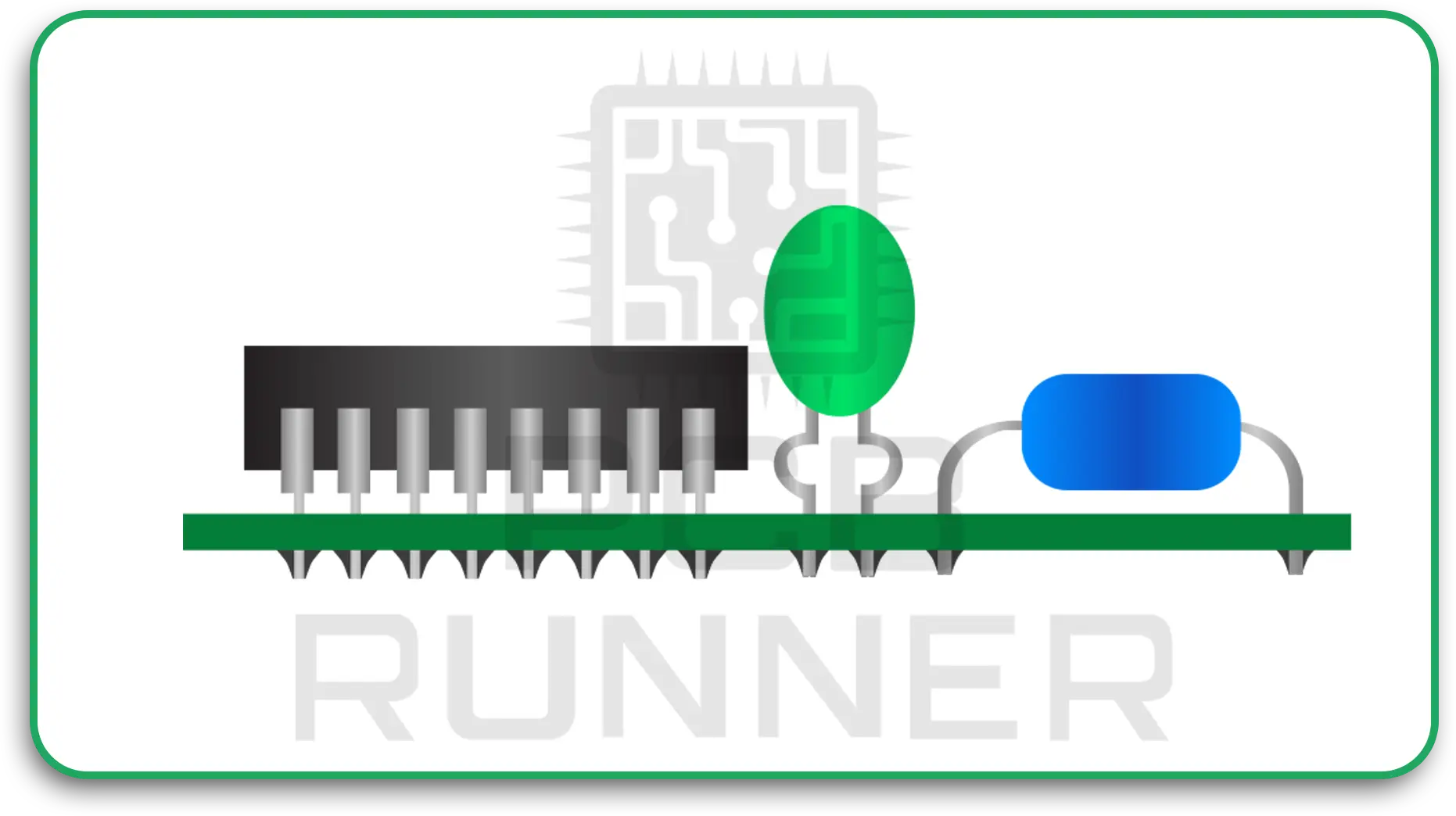
Through-Hole Technology (THT)
This technique includes inserting the component’s leads through drilled holes in the PCB. Although THT is less common among current telecommunications devices, it is still utilized for specific components that need strong mechanical connections.
Multilayer PCB Fabrication
To accommodate routing as well as high-frequency signals, telecommunications PCBs often need multiple layers. Multilayer PCBs are helpful in telecommunication PCB applications due to:
- The greater operational Capability.
- The reduction of electromagnetic interference (EMI).
High-Density Interconnect (HDI) Technology
Modern telecommunications devices need HI PCBs because they allow for the following:
- Miniaturization of electronic components.
- Improved speed of signal transmission.
Controlled Impedance Techniques
Telecommunication requires efficient signal integrity maintenance. This can be achieved by utilizing controlled impedance techniques, which limit communication interference.
Best Practices for Manufacturing Telecommunication PCBs
For optimal results, suppliers must comply with industry standards: Best Practices for Manufacturing Telecommunication PCBs
- Design for Manufacturing: The method involves altering a PCB structure for enhanced efficiency during production.
- Thermal Management: It includes the employment of plastics which have a high-temperature resilience coupled with heat-dissipating metal cores.
- Signal Integrity Testing: Evaluation of all forms of signals for effectiveness.
- Environmental Testing: The board’s functionality is determined by its behaviour in extreme conditions.
Why Choose PCB Runners for Telecommunication PCBs?
For over a decade, PCB Runners have also been known for manufacturing custom-printed circuit boards and PCB Runners for Telecommunication PCBs. The following specifics set us apart:
- Advanced Technology: Our equipment for production is highly sophisticated which allows us to make products with high precision.
- Material Expertise: We have experts who help the client select the right materials appropriate for their needs.
- End-to-End Solutions: We offer services throughout the product’s lifecycle, such as design, programming, and assembly.
- Quality Assurance: All the PCBs are subjected to multiple tests to confirm acceptance of the defined industrial requirements.
Supporting the ever-changing demands of the telecommunication industry ranges from innovation to dependability, which is something we at PCB Runners focus on.
Conclusion
To incorporate high-performing PCBs within devices and networks, one must pay attention to details such as materials and advanced manufacturing techniques.
With the help of experts such as PCB Runners, companies can obtain custom PCBs that can withstand the challenges of telecommunication applications. Call us to learn more details about your upcoming project and see how we can assist you regarding quality and service.
FAQs
Q1: What is a telecommunication PCB?
A telecommunication PCB is a PCB used for communication devices such as routers, antennas, and base stations.
Q2: What materials are commonly used in telecommunication PCBs?
Composites with electrical and thermal properties, such as FR4 metal laminate and RogeRs laminates with a metal core, are popular.
Q3: Why is thermal management important in telecommunication PCBs?
Telecommunication devices produce excessive heat. Thermal management is very important to prevent overheating and ensure proper function.
Q4: What is controlled impedance in telecommunication PCBs?
Controlled Impedance is the strand of controlling the resistance and reactance within PCB traces to ensure signal integrity.
Q5: How do PCB Runners support telecommunication PCB manufacturing?
PCB Runners provide telecommunications PCBs with the latest technology and qualified personnel to make the necessary custom PCBs for telecommunication usage.