Surface Mount Device (SMD) technology has changed the design and assembly of modern printed circuit boards (PCBs) the are designed and manufactured. Compared with conventional components that are assembled by means of a hole, SMD circuit boards are more superior and efficient because they save space unlike their predecessor’s left components. This makes SMD circuit boards most suitable for compact and high-performance electronic devices.
SMD PCB manufacturing is important to know especially if you are dealing with a pcb circuit board manufacturer or you are designing your own multilayer printed circuit board. This guide discusses how SMD boards function, details the steps in SMD PCB manufacturing and provides suggestions on how to design SMD PCBs properly using PCB design software.
What is an SMD PCB?
An SMD PCB is a Circuit Board Assembly where Surface Mount Device (SMD) components are used instead of older through-the-hole components. SMD components are soldered on the surface of the PCB, and there is no need to drill any holes.
Advantages of SMD Circuit Boards
Smaller and lighter: Compact designs can be achieved due to SMD components having a smaller footprint.
Higher component density: A more significant number of components can be accommodated within a multilayer printed circuit board.
Faster assembly: Speed in the production process is enhanced due to the automation of SMD PCB manufacturing.
Improved electrical performance: Signals have lower loss and interference due to shorter leads.
Cost-effective: SMD circuit boards can be built cheaply because they are produced at scale.
How SMD Boards Work
PCBs like SMD Boards have some differences from the traditional to, including the use of smaller mountable parts as opposed to through-hole components. These mountable parts can accommodate high frequencies, so they are used in:
- Consumer electronics like smartphones, tablets and laptops
- Automotive electronics like ECUs and Sensors
- Medical devices such as wearables and implants
- Industrial automation with IoT Sensors and Control units
In SMD PCBs, signals travel through copper traces, which connect the different electronic components. Resistance to Inductance ration is improved with shorter lead lengths which leads to better circuit performance.
SMD PCB Manufacturing Process
A high quality SMD circuit board is a result of precision with advanced technology for PCB manufacturing. Following is the SMD PCB manufacturing process:
Step 1: PCB Design and Prototyping The process starts with an SMD PCB in a PCB design software, which includes Altium, Autodesk Eagle and KiCad. Engineers make sure Components are placed optimally; Signal interference is minimal, and Trace routing Thermal management is done. The final design allows for a prototype to be made so it can be tested.
Step 2: Producing the Printed Circuit Board
In this phase, the layers of the Printed Circuit Board (PCB) are created, which consist of the following processes:
- Etching of copper traces on the board
- Solder mask application for protective reasons
- Component label printing on the silkscreen
Step 3: Automated Application of Solder Paste
Solder paste is deposited on the pads fitted with a stencil to secure where the components are going to be mounted. The paste contains a mix of tin, silver, and copper in order to provide strong electrical connections.
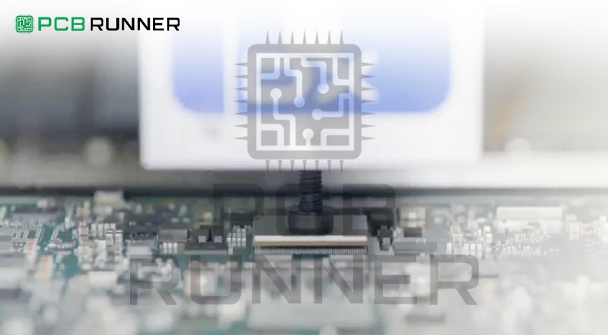
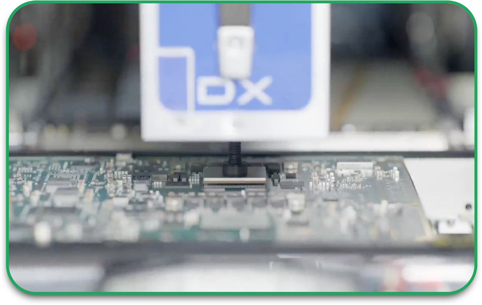
Step 4: Use of the Pick and Place Machine
Precision mounting of surface mount devices (SMD) components onto the printed circuit is done by rapid robotic arms. This process is automated, which gaurantees precision and effectiveness which leads to proper mass production.
Step 5: Solder Reflow
After mounting, the PCB assembled undergoes solder reflow. It is when the PCB assembled is heated in a refractable oven, which liquefies the solder paste to secure the components in the proper position. By controlling the temperature appropriately to prevent overheating, excessive damage to the delicate SMD components can be avoided.
Step 6: Evaluation and Analysis
The quality control tests that PCB undergo after assembly involve these three phases:
- Automated Optical Inspection (AOI): Analysis and recognition of visible defects in soldering as well as(device misalignment)
- X-Ray inspection: Determine the solder joints concealed beneath components like Ball Grid Arrays (BGAs)
- Functional Testing: Ensures that proper circuit performance occurs before final assembly.
Step 7: Wrap-Up of Assembly and Product Distribution
Post-test, the assembled Surface Mount Device(SMD) circuit boards are incorporated into the final product, put into a package and forwarded to the customer.
How to Design SMD PCBs – A Guide
When designing SMD circuit boards, best practices are followed for optimal performance and board reliability. Here is a step-by-step breakdown of how to design SMD PCBs
Choose the Correct PCB Layout
Software Printed circuit board design software is used to construct the PCB layout. Some of the most common include: – Altium Designer- Best suited for specialized designs – KiCad- Open-source version is handy for beginners – Eagle – Commonly used for both industrial and hobbyist PCBs
Improve the Component Placement
Ensure that high-frequency components are placed together to reduce signal loss. Sensitive circuits should be placed further away from heat-generating components. Separately position power and ground planes to maintain stability.
Create a Designed Trace Routing
Draw direct traces without reducing resistance. Ensure uniform current flow by maintaining consistency in trace widths. Signal reflection is prevented by avoiding 90-degree angles in traces.
Manage Thermal Control
Invest in thermal vias close to power components. Increased dissipation of heat is accomplished by using heat sinks or copper pours.
Choose Correct Solder Mask
Solder mask protects PCB from oxidation and solder bridging. Do a PCB circuit board manufacturer search and select one that uses high-quality solder masks to ensure durability.
SMD PCB vs. Through-Hole PCB: Which One is Better?
While SMD circuit boards dominate modern electronics, through-hole PCBs still have some advantages. Let’s compare them:
| Feature | SMD PCB | Through-Hole PCB |
| Component Size | Smaller, compact | Larger, bulkier |
| Assembly Speed | Fast (automated) | Slow (manual or wave soldering) |
| Mechanical Strength | Less durable | Stronger for high-stress environments |
| Cost | Lower for mass production | Higher due to manual labor |
| Signal Performance | Better for high-frequency circuits | More resistance and interference |
For most applications, SMD PCBs offer better performance, lower cost, and faster production. However, through-hole technology is still used for high-power and high-reliability applications like aerospace and military systems.
Essential Considerations When Selecting a PCB Manufacturer for SMD Boards
Finding a reliable PCB manufacturer is the first step in getting quality SMD circuit boards. Consider the following:
Manufacturing Capabilities
- Can they manufacture multilayer printed circuit boards?
- Can they execute High-Density Interconnect (HDI) technology?
- What are the quality standards that they practice?
Prototyping Services
- Do they provide rapid turnaround prototypes for pre-production testing?
- Are they able to produce both small and large-volume orders?
Quality Control
- Do they use Automated Optical Inspection (AOI) X-ray and Functional Testing?
- Do they comply with ISO and IPC quality standards?
Customer Service
- Do they respond promptly to redesign requests?
- Do they provide DFM (Design for Manufacturing) services?
With PCB Runners, you get SMD PCB manufacturing services and impeccable quality circuit board assembly for all types of businesses around the globe. From developing prototypes to mass production, we provide dependable, low-cost options.
Expert Insights
Surface Mount Technology (SMT) has transformed the electronics industry by making devices smaller, lighter, faster, and more affordable. Unlike older methods, reflow soldering has become the preferred technique because it provides higher efficiency, reliability, and better manufacturing results compared to wave soldering.
To meet the demand for compact and high-performance electronics, area array packages have replaced traditional designs. These packages offer higher input/output (I/O) density, improved manufacturability, and better speed while reducing the overall size of components.
SMT components, known as Surface Mount Components (SMCs), are widely used in electronics. They include capacitors, resistors, transistors, diodes, inductors, integrated circuits (ICs), and connectors. However, due to their small size, most SMCs can only handle power dissipation of 1 to 2 watts.
These components are mounted onto Printed Circuit Boards (PCBs) using different methods like solder paste reflow, wave soldering, or conductive adhesive curing. While conductive adhesives are less common, they are used in flexible circuit boards or for heat-sensitive components. SMT continues to be a key technology in modern electronics manufacturing.
Final Thoughts
The introduction of SMD circuit boards is constantly changing the electronics industry with smaller, faster, and better devices. Knowing the SMD PCB manufacturing procedure combined with the best methods of how to design SMD PCBs will lead to enhanced performance and reliability.
Searching for a reliable PCB manufacturing company? Look no further; PCB Runners specializes in custom-printed circuit boards and high-precision SMD assembly. Reach out today for expert assistance with PCB fabrication and circuit board SMD assembly.
Frequently Asked Questions (FAQs)
What is SMD PCB?
An SMD PCB is a printed circuit board that incorporates surface mount devices in place of traditional through-hole components.
How does SMD PCB manufacturing work?
The process comprises fabrication of the PCB, solder paste application, placement of components, reflow soldering, and quality inspection.
Which software is the most effective to use for designing SMD PCBs?
The most popular choices would be Altium Designer, KiCad and Eagle.
What are some benefits of SMD PCBs compared to through-hole PCBs?
SMD boards are smaller, faster, cost effective and can accommodate greater component density.
Where can I find quality SMD PCB fabrication?
For expert SMD PCB fabrication and circuit board assembly, contact us today at PCB Runners.