Smartphones, laptops, TVs and smart watches, nearly every room today is filled with electronics. It is wondrous to think, what is next? Innovations in design, new materials, and technology shifts are moving the electronics world at full speed. In this blog, we are going to explore the key trends, remarkable innovations, and essential factors regarding the future of electronics. Also, we will encapsulate how innovative technology is leading us to a greener future, along with the advanced manufacturing processes of tiny circuit boards.
The electronics industry is growing at an astonishing pace. It is anticipated to be worth hundreds of billions of dollars with an ever-increasing smart device and aid bazaar. From grocery lists to talking with your refrigerator, we already have smart devices with almost limitless capabilities. The future holds cars that drive themselves and early illness-detecting tiny devices for medical applications.
As the industry shifts, designers, users and those that rely on these devices are in for a remarkable surprise. Let us explore what is on the horizon and what that means for the common folk. From extraordinary healthcare devices that are implants to robotics and AI-integrated vehicles, the future of electronics remains limitless.
The PCB: Understanding Electronics as a System
At the heart of all modern electronic devices, such as smartphones and car dashboards, printed circuit boards (PCBs) serve a critical role as the “nervous system” of any device. Just as the nervous system integrates and orchestrates activity throughout an organism, PCBs connect and integrate all the device components. For the more complex devices like medical devices, PCBs play an equally critical role in performing and ensuring the device functions accurately and effectively.
Why PCB Technology is Imperative to Electronics
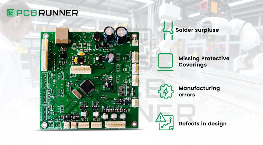
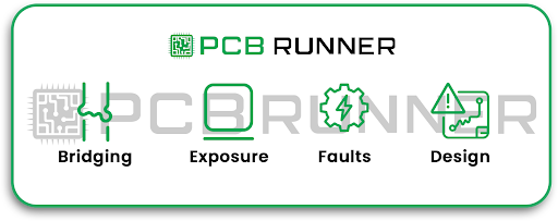
- Reliability: All electronic devices, such as smartphones, must serve their intended purpose at all times.
- Advanced miniaturisation: As modern electronics shrink, PCBs are required to integrate components into a shrink in footprint.
- Custom Designs: As the diversity in the population changes, the device functionalities must serve the needs of the modern-day individual.
- Sustainability: Business and manufacturing of electronics are shifting towards employing fewer materials and zero-waste manufacturing.

Innovative Trends in PCB Manufacturing
Innovation trends in PCBs are meant to capture the interest of electronic enthusiasts. To capture the interest of electronic enthusiasts, the leading manufacturers of PCB circuit boards are going beyond ‘green boards’ by using unique materials and advanced modelled structures to create broader and more complex functions.
1. 3D Printing and Prototyping
Picture this: you can now print a customised circuit board nearly as effortlessly as printing a photo. 3D printing boosts productivity and improves the rate at which concepts are turned into products while reducing waste.
This accelerates the journey from inspiration to implementation and accelerates market availability.
2. Smarter Automation and Robotics
Faster output and quicker inspection of tiny chips and boards is now possible with robotics.
This translates to improved accuracy, less rework, and quicker availability in the market.
3. Rigid Flex and Rigid PCBs: Flexible, Yet Strong
These are used to manufacture thin and lightweight gadgets, including wrist watches and hearing aids. Smartwatches are also designed using this technology.
The reason why fitness trackers and phones are slimmer and can even bend is due to rigid flex PCB technology. This technology combines rigid sections that provide toughness with flexible sections that are able to assume different and intricate shapes.
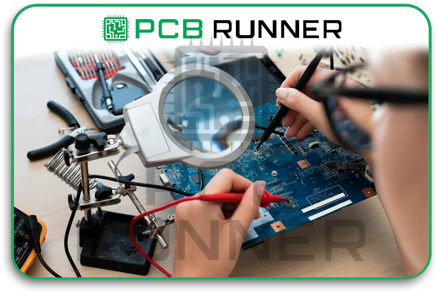
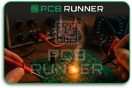
Electronics PCB Assembly: Improving Efficiently Each Day
After assembling and preparing the board, the next step is to incorporate its components: the connectors, sensors, and chips. Here is the update that the PCB fabrication assembly is receiving:
- Surface Mount Technology (SMT): Specifically for miniaturised chips, it is encapsulated and placed on the surface, allowing your devices to perform more advanced feats while maintaining a small and compact silhouette.
- Advanced Materials: Graphene and ceramics are shifting the gadgets industry and allowing the products to have a longer life span. A device, even when used nonstop, will continue to run cooler.
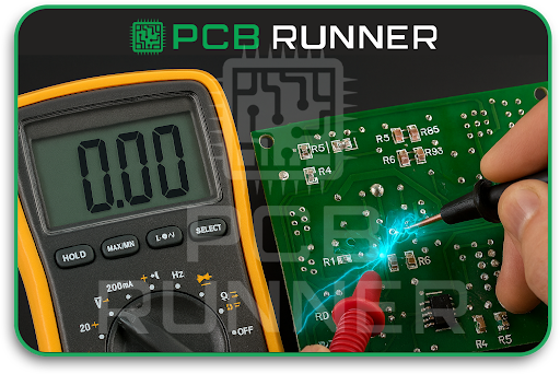
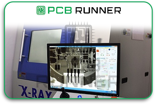
Smart cameras and sensors are able to perform more complex and advanced inspections. Devices with such automated inspections have higher quality standards.
Global Trends: What’s Powering the Future?
There is more to the devices than “smaller and portable”. These macro changes are the foundation for the outlook of electronics:
1. The AI and IoT Revolution
Smart devices are becoming more commonplace, and the forecast for IoT devices is beyond 25 billion.
Artificial Intelligence is ubiquitous and growing rapidly. AI is integrated with phones, cars, or even homes and self-optimises based on learned usage patterns.
2. Sustainable and Green Design
A common industry trend is to be more eco-friendly by utilising non-harmful materials and increasing recycling. Thus, the processes of manufacturing PCBs and other electronics decrease pollution and save energy.
“Green” technology will be a common sight in your homes shortly.
The arrival of a new mobile network, 5G, will allow for linked appliances to communicate with each other in real time, thus making your smart home and car operate with even better efficiency.
3. Medical, Automotive, and Aerospace enabled with technology.
Miniaturised PCBs allow for the use of advanced devices like hearing aids and cardiac monitors, thus helping the patients live better lives.
High-grade boards from dependable manufacturers are crucial to the safety, reliability and dependability of the automobile, aeroplane and even rocket for every journey.
Tips:
- Don’t forget to move your wearable gently.
- How to choose the right PCB Type for your device
- In case of space constraints, a rigid flex PCB is best for medical wearables and ultra-small devices.
- For managing heat, the use of advanced materials like ceramics is effective in keeping the boards cool.
- For the quickest possible assembly, look for automated electronic assembly manufacturing. It can sharply reduce the waiting period for your job.
The Human Side: What Does This Mean For You?
As for everyday users, you are looking forward to more powerful, reliable, and sustainable technology. Electronics are designed to seamlessly integrate into your life, making daily tasks easier, enhancing safety, and providing seamless connectivity.
Looking forward, the world is changing. Boundless possibilities are waiting for youngsters ready to dream up the next gadget. Starting is simple and requires little to no investment; now is the time to jump in, experiment, and create.
Looking Forward: What’s Next for PCB Manufacturing in the UK and Beyond
The rise in PCB production in the UK and the rest of Europe is powered by unique combinations of traditional skills and new ones. In the medical, defence, and aerospace sectors, businesses demand absolute precision and zero mistakes and expect faster tech support, seamless communication, and full-service manufacturing, all in one place.
As things continue to shrink and become smarter, the sophisticated PCB designs and rigid flex circuits will consistently evolve further. Enhanced automated processes, eco-friendly measures, AI incorporation, and instant quality assessments all paint a positive picture, and a dependable future, for those who rely on electronics.
Conclusion: Adopting the Collaborative Approach
The world of electronics is ever-evolving. It all began with the first PCB and now includes cutting-edge wearable technology and smart factories. We continue to strive forward with endless innovation.
Supporting high-tech medical equipment and smart gadgets with regular and smart gadgets, PCB Runner and other companies have been leading the field for over a decade now. The new shift will further evolve with global changes, consumer needs, and the increasingly high desire for the ultimate device.
If you are interested to learn more, now is the perfect time to explore electronics and PCB technology and witness the changes being forecasted for the near future.