The integration of electronic components into a single device has escalated the need for dependable multilayer printed circuit board (PCB) testing. These boards serve as the foundation for contemporary electronics, containing complex connections and components within several layers.
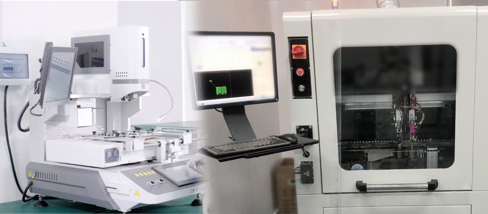
The operation of these devices is fault-free only after adopting sophisticated testing methods. Automated X-ray inspection (AXI) is increasingly being used and has developed into an essential gear for testing these devices upon completion. This article highlights how automated x-ray inspection PCB performs, its benefits, and how it allows for stringent control of checks.
The Complexity of Multilayer Printed Circuit Boards
Multilayer PCBs are key to most advanced applications, such as telecommunications, aerospace, automotive, and even healthcare devices. With several conductive layers encased in insulating material, these boards have improved function and performance. However, the level of sophistication of these boards brings forth problems during the manufacturing stage. These problems include hidden solder joint defects, component misalignment, and via-incomplete stages.
Advanced testing techniques such as optical inspection and electrical testing seek to overcome these challenges. Unfortunately, neither approach is adequate for addressing the possible multilayered internal defects hidden inside the PCB. Hence, automated X-ray inspection PCB can prove to be a significant advancement in the industry.
How Automated X-Ray Inspection PCB Works
AXI systems harness high-energy X-rays to penetrate through and reveal the internal structures of a PCB. Unlike visual inspection, which only looks at the surface, X-rays can expose hidden defects located within the board’s layers. These systems create sophisticated images displaying the quality of solder joints, the placement of components, and other possible defects.
Typically, the procedure consists of the following stages:
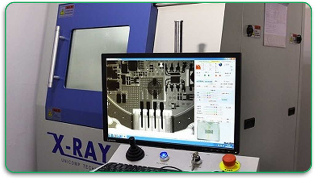
- Image Acquisition: Capturing images at pre-defined angles using X-ray projection on the PCB.
- Data Interpretation: Using X-ray imaging to perform defect recognition with artificial intelligence algorithms.
- Defect Recognition: The system captures voids, missed alignments, and solder bridging as problems highlighted by the system.
AXI is especially effective in discovering defects in Fine-Pitch Components and High-Density Interconnects (HDI) because those flaws are difficult to see with the naked eye.
Expert Insights: Enhanced Testing Techniques
As noted in an article from ResearchGate, older X-ray techniques such as Digital Radiography (DR) often struggle with multilayer printed circuit board testing. Overlapping images provided by DR makes patient diagnosis very challenging since it becomes impossible to view every layer distinctly or to find clear defect locations.
To overcome the previously described issues, the study proposes an innovative technique that uses the following steps:
- Oblique Angle Irradiation: The surface of the PCB is irradiated with X-ray at an angle that is not perpendicular to the surface.
- Rotational Projection Imaging: The board undergoes rotation while projection images are taken.
- Slice-by-Slice Reconstruction: Each layer of the image is constructed from detailed cross-sections revealing pertinent information for every single component of the target object.
This approach remarkably boosts the overall accuracy of defect analysis and provides insight into the construction of the PCB’s internal layers.
Advantages of Multilayered PCB X-Ray Inspection
1. Non-Destructive Testing
The primary benefit of automated X-ray inspection PCB is completely damage-free inspection. Manufacturers can examine PCBs without the risk of inflicting any damages that would hinder repair or rework.
2. Enhanced Defect Detection
A very diverse number of defects can be widely identified using X-ray inspection, including but not limited to:
– Voids in solder joints.
– Missing or misconfigured components.
– Inadequate or improperly constructed vias.
– Short circuits or solder bridges.
3. Improved Quality Control
X-ray inspection reduces defect and scrap rates, resulting in improved overall product reliability by catching mistakes earlier in the production cycle.
4. Automation for Efficiency
Quality remains high while meeting the demand of a high volume of production due to rapid and accurate testing provided by automated X-ray systems.
5. Layer-Specific Analysis
Other techniques than traditional methods offered detailed layer-specific analysis and the ability to gain insights not previously accessible. This research gate study has covered the machine learning reconstruction method, for example.
Use of PCB X-ray Manufacturing Process
Xray technology, particularly AXI, is used at almost all stages of PCB manufacturing:
- Prototyping: A step that validates that a design does not have any glaring mistakes at the start.
- Mass Production: Doing production in bulk with a guarantee of consistency in the quality of output.
- Defect Investigation: Determining the reasons and failure parts for the PCBs found to be defective.
Aerospace, telecommunications, and automotive industries are big users of the technology due to established quality requirements.
From Supreme Materials to PCs: Testing with a Challenge
As bulk production of PCBs becomes commonplace, testing becomes increasingly challenging, which is one reason why advanced materials have to be properly tested. As devices become smaller and more powerful, materials like solder masks and high-frequency laminates create big problems.
AXI systems will have to change to improve the materials that can be inspected on judgeable terms. Quality monitoring and check-ups of non-conductive or super-dense layers will be the basic requirements for ensuring quality maintenance.
New Agendas in Xray Inspection Technologies for PCBs
1. 3D X-Ray Imaging
Level and volumetric data that can be attained with newer 3D X-ray technologies allow for extremely accurate analysis of complicated structures.
2. AI Based Analytic
Along with more profound levels of scrutiny, the use of artificial intelligence and machine learning for automated X-Ray Inspection systems in ramping up deficiency distinctions, while keeping the rate of false alarmers in check.
3. Smarter Automation
Improvements in automation will be made in future systems, further boosting the inspection speed while minimizing the need for operator involvement.
Conclusion
Methods such as automated X-ray inspection (AXI) are necessary. To achieve higher precision in multilayer PCB testing, TX-ray inspection nondestructively examines the internal structures of modern PCBs, which determine the reliability and functionality of contemporary electronic devices.
PCB Runners is a well-known provider of comprehensive PCB solutions and offers design, manufacture, and testing services. Our experience in multilayer PCB production and new inspection methods guarantee that our customers receive dependable, high-quality products.
Give us a call today to discover how we can assist your next project by utilizing these advanced PCB solutions.
FAQs
1. What is a multilayer printed circuit board?
A multilayer printed circuit board (PCB) has more than one conductive layer with insulating materials in between the layers; these PCBs offer enhanced functionality for more sophisticated electronic devices.
2. What exactly is automated X-ray inspection (AXI)?
AXI helps visualize the internal structure of PCBs using X-rays, which makes defect detection easier as defects are concealed within the assembly structure, hence improving the quality of the product.
3. Why is multilayer PCB’s X-ray inspection so important?
X-ray inspection can capture defects obscured by external layers and is necessary for ensuring product reliability and high endurance performance.
4. What do you think the defect AXI can reveal?
AXI can detect voids in solder joints, misplaced components, incomplete vias, and short circuits.
5. What goes into the maintenance of quality in multilayer PCB production provided by PCB Runners?
Runners PCB uses the latest inspection efforts, like AXI, to keep its quality standards at a high level and produce reliable PCB solutions.