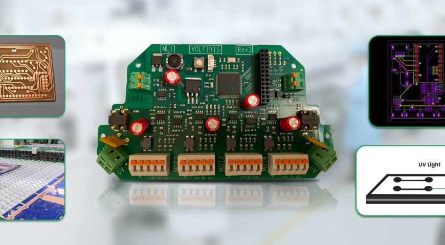
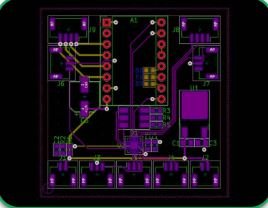
When it comes to making a printed circuit board (PCB), one of the crucial components is etching. Etching removes unneeded copper from the surface of the board, with only needed conductive pathways left. Without Silicon PCB etching, circuits will be non-functional, and their dependability will be at risk.
For manufacturers, picking the right etching method defines the cost, durability, and performance of the board. Understanding these principles is essential whether you are designing a high-density interconnect (HDI) PCB, a very basic multilayer PCB, or even a prototype.
The various methods used to etch PCBs will be explained and compared in detail in this blog, helping you to determine the most useful method for your manufacturing needs.
What is PCB Etching?
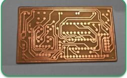
Etching is part of the PCB manufacturing process, where copper is removed from the surface of a PCB circuit board, creating the appropriate traces made of the conducting material. This step occurs only if a resistance layer (a layer that covers the PCB) has already been placed on the board. The copper that was not protected by the resist layer will be removed by the etched solution, leaving the intended paths for the circuitry.
Etching must be done with accuracy as unregulated etching can lead to over-etching, undercutting, or a non-uniform width of the trace, all of which affect circuit performance negatively.
Step-by-Step PCB Etching Process
Preparing the PCB
- At the start of the etching process first stage of etching is to clean the copper-clad board of any oil or oxidation.
- This helps with the adhesion of the protective layer, much as a 10-second adhesive will make adhesion for the protective layer easier.
Application of the Resist Layer
The next stage involves shielding the whole board with a protective photoresist, which can be liquid resist or dry film resist. It covers some surface of the shielded copper so as to create the desired circuit design.
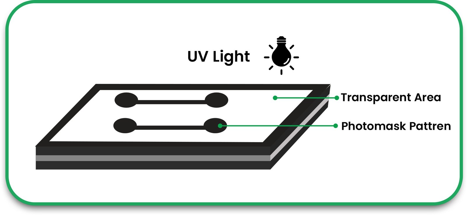
Circuit Pattern Exposure
The circuit pattern is printed onto the board using a laser imaging technique or a UV light source. The unprotected areas of the shielded copper are left exposed for etching.
Etching Method Selection
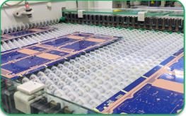
At this stage, some of the copper that had been shielded is taken away with one of the copper PCB etching processes. The most suitable one varies depending on the complexity and costs of the board alongside the accuracy that is needed.
Clean the Board and Strip the Resist
After the etching process, the passive photoresist that is left over is stripped away, exposing the copper traces to view. The last process is to clean the circuit board from any materials it has left.
Post Assessment Quality Control
The PCB circuit board manufacturer inspects the fabricated board for precision in relation to the specifications individually set, checking that there is no excessive etching or lack of expected traces.
Etching Method Varieties for PCB
Chemical Etching Wet Method
Dissolving copper by use of liquid chemicals is the most usual technique used in PCB fabrication and hence, is ths most used method for PCB fabrication.
Common Solutions for Wet Etching:
- Ferric Chloride (FeCl3): Widely used option due to its low price, but it needs the proper disposal of waste.
- Ammonium Persulfate: Cuts edges cleaner, ideal for fine-line circuits.
- Alkaline Etching (Ammonia Based): Used for High-Density InterConnect (HDI) PCBs because of high accuracy.
Wet Etching Pros:
- Monetary efficiency for bulk production.
- Applicable for multilayer and single-layer PCBs.
- Simple to execute in basic PCB shops.
Wet Etching Cons:
- Possibility of undercutting (chemicals spreading beneath the resist).
- Needs special treatment for waste disposal.
- It’s not as accurate as dry etching for advanced circuits.
Dry Etching (Plasma or Ion Etching)
Copper is removed by plasma or ion beams with dry chemicals instead of liquids. It is accurate and is often applied to HDI PCB technology.
Common Dry Etching Techniques:
- Plasma Etching: Dismantles copper with reactive gases without harming tiny features.
- Ion Beam Etching: Physically removes copper with a focused ion beam for extreme precision.
Pros of Dry Etching:
- Great for accuracy-required processes, such as HDI PCBs.
- No possibility of chemical undercutting.
- Environmentally safe (no liquid waste to dispose of).
Cons of Dry Etching:
- Equipment and processing are costly.
- It’s not as fast as wet etching for large quantities.
- It is not commonly found in smaller PCB shops.
Comparing PCB Etching Methods: Wet vs. Dry Etching
| Feature | Wet Etching | Dry Etching |
| Cost | Lower | Higher |
| Precision | Moderate | High |
| Environmental Impact | Requires chemical disposal | More eco-friendly |
| Best for | Multilayer PCBs | HDI PCBs and fine traces |
| Processing Speed | Faster | Slower |
For most pcb circuit board manufacturers, wet etching is the preferred method due to its cost-effectiveness. However, if you’re working with HDI flex circuits or ultra-fine traces, dry etching may be the better choice.
Challenges in PCB Etching and How to Avoid Them
- Undercutting (Loss of Trace Width)
Issue: More copper is removed than desired because chemicals flow underneath the resist layer.
Solution: For better control, use plasma etching.
- Over-etching (Excessive Copper Removal)
Issue: Missing traces due to severe over-etching.
Solution: Never loosen up on monitoring etching time and the strength of the solution.
- Inconsistent Etching (Uneven Copper Removal)
Issue: Remove copper with varying thicknesses to form a circuit.
Solution: There should be uniform exposure at the essence of controlled etching baths and some level of abrasive methods.
- Environmental Issues
Issue: Damage caused to the atmosphere due to inaccurate elimination of etched chemicals.
Solution: Move towards dry etching or safe chemical disposal methods.
Etching for High-Density Interconnect (HDI) and Multilayer PCBs.
Wet etching is typically most preferred for PCBs due to the cost-efficient method, but pours it to these boards; these boards are also a more layered, more power-packed version of traditional boards. Conventional wet etching is inefficient for aimless etching due to fragile lines, micro vias, and multilayers as well.
Plasma etching is regarded as the most preferable option because of its incredible capability to etch intricate details.
Signal integrity for multilayer PCBs demands etching consistency between layers. PCB etching services usually employ a combination of wet etching for large areas and dry etching for fine-line circuits.
Expert Insight
Etching is a technique of PCB fabrication where copper is removed from a laminated board using a defined acid due to the negative image printed over copper. If done manually, it is time-intensive, does not scale well for large board sets, and can get very dirty. Moreover, some of the etching solvents can also be harmful to the user’s well-being.
Machines have better precision and speed when it comes to etching, and they can simultaneously process many boards in a row; however, for many small PCB manufacturers, they are still too expensive. To solve this, automated etching systems offer a safe and simple method for carrying out the etching sequence with minimum user interaction.
A PCB serves the purpose of supporting and electrically connecting various components with conductive tracks, pads, and outlined shapes made of copper foil which is affixed to a dielectric substance. This eliminates user error and provides manufacturers with low-cost solutions during PCB etching.
Future of PCB Etching Technology
With more complex designs, modern PCBs and their etching technologies are changing. The following list is some trends to monitor:
Ultra-Precise PCBs Flex and rigid etched geometries are best achieved through laser etching. Eco-Friendly Solutions Etching chemicals used in PCB manufacturing are becoming less hazardous. Automated Systems AI etching machines enhance quality and lower error rates.
Conclusion
The PCB etching process is a fundamental step in PCB fabrication, directly impacting the quality and reliability of circuit boards. Whether you choose wet etching for cost efficiency or dry etching for precision, selecting the right PCB etching method ensures optimal performance for your application.
For high-density interconnect (HDI) PCBs, dry etching techniques provide superior results, while multilayer PCB manufacturers often rely on controlled wet etching for cost-effective production.
Looking for a trusted PCB manufacturer with advanced etching capabilities? Contact PCB Runners today for expert guidance and high-quality PCB fabrication services!