Optimising PCB Design: Counterbore vs. Countersink

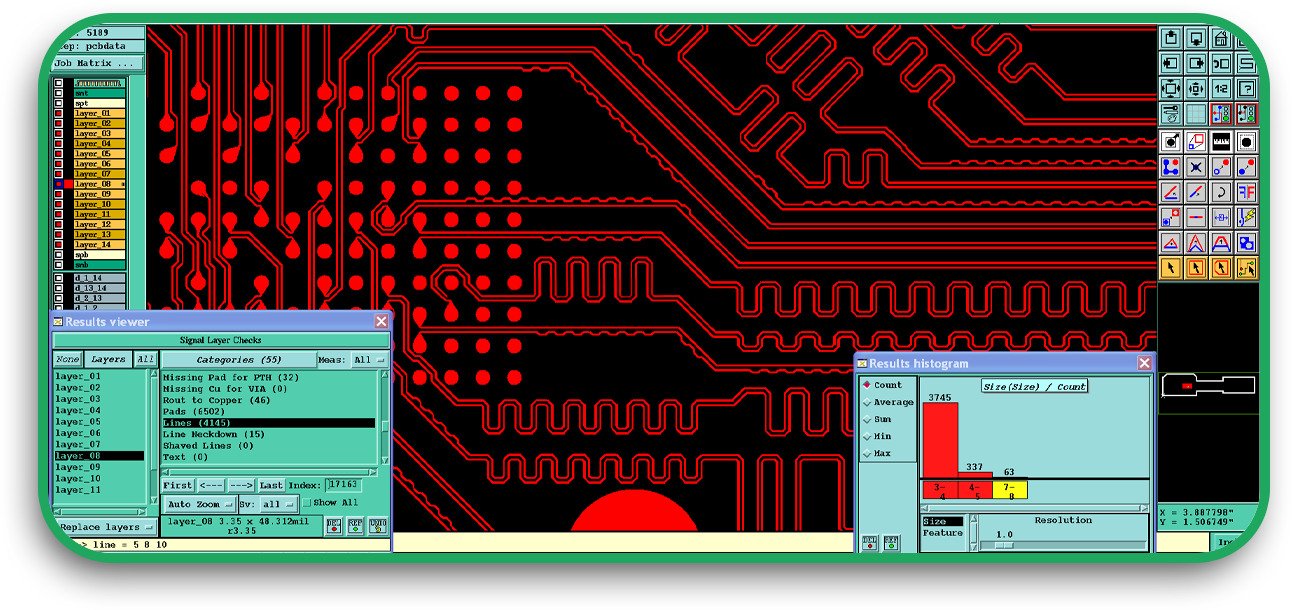
While developing multilayer PCBs, an engineer has to consider each part of the board, including hole types. The two types of holes that PCB circuit board manufacturers most commonly use are counterbore holes and holes with countersink features. These holes affect the positioning of fasteners and other components and, therefore, the board’s reliability and structural strength.

Understanding the differences between counterbore holes and holes with countersink features is necessary to make a design choice. In this blog post, I will outline the features of these holes, how they are applied, and the details of crafting PCBs for multilayer PCBs.

Optimising PCB Design

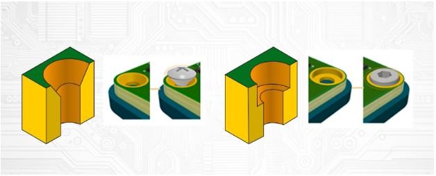
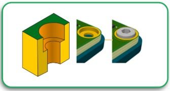
Explaining Counterbore Holes in PCBs

A counterbore hole is a type of hole that has been modified such that the inner face is straight, and the base is flat and cylindrical. Counterbores are common in the industry of PCB manufacture with mechanical fastening as a requirement, whereby the bolt or screw head rests above, continues to be adjusted and allows a general size of tightening within the PCB.
Counterbore Holes

Benefits of Counterbore Holes

  • Stable Fastening: Counterboars guarantee that screws and bolts are busy fastened appropriately without disruption.
  • Ideal for Thick PCBs: Frequently used in multilayer PCBs, the components of which need to be secured mechanically excessively.
  • Counterbore holes can be used for the following: reinforcement designs in the structure that needs the use of machine screws or bolts. For securing heavy components in PCB fabrication. For the use of screws that need to be flush mounted onto the surface of the PCB.

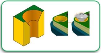
Like with a conical hole, a screw countersink is a cut that permits the screw to be flush with the surface of the PCB. The angle of a countersink is cut to be the same as the head shape of the screw, providing a smooth shift from the screw to the board.

Having countersunk screw holes brings a lot of advantages, such as Aesthetic and design function: It provides smooth covers that do not leave exposed protrusions that can get snagged accidentally. Perfect for thin printed circuit boards: Functions perfectly on thinner boards, barring the use of a counterbore which results in excessive material removal. Improved mechanical strength: Increases stiffness by lowering stress concentration through more evenly distributing force across the PCB.

For printed circuit boards that have limited space, the use of a hole countersink is ideal. Additionally, with the Read-along, face-mounted components eliminate a lot of external protrusion and butt joint screws that are to be sunk into the surface of the board.

How to Decide Between Counterbore and Countersink When Designing a PCB

1. Take PCB Thickness into Consideration

Counterbore holes are more appropriate for working with multilayer PCBs due to the added support they offer. Custom-printed circuit boards benefit more from hole countersink features, as they require less material removal.

2. Review The Needs of Components and Fasteners

If your design has bolts or machine screws, then use a counterbore hole option. If your design utilises flat-head screws that need to rest flush to the surface, you should use the hole countersink option.

3. Consider The Level of Structural Integrity Required

Counterbore holes should be used for added durability in high-stress environments. Hole countersinks work best for applications that require smooth surfaces.

Countersink

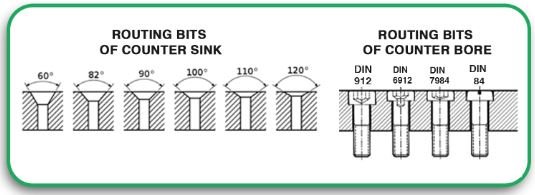
Key Differences Between Counterbore and Countersink Holes in PCBs

Feature Counterbore Hole Hole Countersink
Shape Cylindrical with a flat bottom Conical with a tapered angle
Best for Thick, multilayer PCBs Thin PCB fabrication
Fastener Type Machine screws, bolts Flat-head screws
Load Distribution Evenly spreads mechanical stress Helps align and secure components
Common Applications Industrial PCBs, heavy components Consumer electronics, aesthetic designs

Counterbore vs. Countersink

Most Important Tips For The Integration of Counterbore and Countersink Holes in PCB Designs

Integrate Counterbore or Countersink Holes using Standard PCB CAD Software.

Aim for precision and accuracy when integrating counterbore or countersink holes in your design. Using standard PCB CAD software is important when aligning components to holes or specifying the depth of the holes.

Confirm Hole Depth

Whether you are designing multilayer PCBs, thin boards, or custom boards, correct tolerance and hole depth should be sufficient. Always consult with the State’s PCB circuit board manufacturers to confirm that they meet the criteria.

Enhance Manufacturing Efficiency

The decision on whether to select counterbore or countersink features must also consider PCB fabrication cost and time. Drilling a perfectly operational hole might involve an additional complication that would increase the charges and lead time for construction.

Test Prototypes For Optimal Results

Producing a printed circuit board prototype enables the designer to analyse the effect of counterbore or countersink holes on assembly practices prior to any large production run.

Expert Insights

This paper describes a mechanical model that attempts to forecast the behaviour of various screw lap shear joints with the aid of a spring-mass model. The spring-mass approach incorporates the axial, bending, bearing, and Shear components of stiffness as well as the masses at the joint. The springs of the model characterise the stiffness resulting from each deformation that occurred. We show how the other components spring-mass model can be simplified. We demonstrate that the joint stiffness we identified can allow for the mechanical behaviour of counterbore and countersink screw lap joints to be observed. We did experimental validation in nine observably different joint positions. The different configurations of the joints are also modelled with the aid of linear finite element methods. In addition, the effect of the individual stiffness components on the total joint behaviour can be investigated by changing the plate’s height and width.

Conclusion

The counterbore and countersink features are both important in PCB fabrication and assembly. The choice of using one rather than the other will rely on the thickness of the board, the type of fasteners used, and the structural strength that must be achieved. Counterbore holes are typically advantageous in multilayer PCBs that have heavy components, while hole countersink features are often needed in custom thin-printed circuit boards for a flush fit.

These differences are crucial for optimised designs that function properly and meet the mechanical requirements of reliable PCB circuit board manufacturers. The appropriate hole type should be chosen in the early stages of development, whether it is a prototype or mass production, to achieve the best performance with little difficulty in fabrication.

Need Expert PCB Solutions?

Are you in need of high-quality PCB fabrication with optimised hole designs? Contact us through PCB Runners today to discuss your industrial PCB manufacturing needs!

The Role of PTH Technology in High-Reliability PCB Designs

These days, almost every electronic device uses a printed circuit board (PCB). New technologies are constantly emerging, and with them, the demand for advanced PCBs rises, particularly in the aerospace, telecom, and medical device sectors.

One of the most commonly used technologies for achieving strong and durable connections is the Plated Through-Hole technology (PTH).

This article compares PTH technology with other advanced methods of making custom-printed circuit boards, such as HDI circuit boards and their PTH counterparts. It also details the key features of custom-printed circuit boards and their durability with PTH technology.

PTH Technology in High-Reliability PCB Designs

What is PTH Technology?

With PTH Technology, an entire PCB assembly is utilized, where holes are drilled through the board and plated with a specific metal to create sturdy electrical connections between the board layers. This type of assembly allows for proper soldering of leads through the board using components equipped with leads.   

How PTH Works

Drilling: The PCB is drilled with mechanical drills that create precise holes.

Plating: The inside walls of the holes are coated with conductive materials like copper.

Insertion of Components: Components with leads are placed through sufficient holes.

Soldering: A soldering iron is used to solder the leads for a secure connection both electrically and mechanically.

Types of PTH PCBs

Single-Sided PTH PCB: The is used in basic circuit designs only.

Single-Sided PTH PCB
Double-Sided PTH PCB: The components are placed on both sides of the board, increasing the circuit’s complexity.

Double-Sided PTH PCB

Multi-Layer PTH PCB: Enhanced features with multiple interconnected layers for a complex, highly efficient multifunctional task.

The Merits of PTH Technologies

Durable Connections: Ideal in applications with high stress, these connections are mechanically rigid and have reliable electrical contact.

Multi-layer Interconnects: Allows for the effortless interconnection of different layers of a custom printed circuit board and its components.

Superior Heat Endurance: Endure highly high temperatures which are prevalent in the industrial and automotive sectors.

Dependable In-Higher Current Applications: Superior current bearing capability in comparison to surface-mounted devices.

Easy Assembly: Suitable for wave soldering and other forms of automation soldering processes.

PTH Technology vs. HDI Circuit Boards

While PTH technology has been a standard for years, High-Density Interconnect (HDI) circuit boards offer an alternative for modern miniaturized electronics.

Key Differences

Feature PTH Technology HDI Circuit Boards
Connection Type Plated through-hole Microvias & blind/buried vias
Board Density Lower Higher (supports compact designs)
Electrical Performance Standard Enhanced signal integrity
Manufacturing Cost Moderate Higher due to advanced processes
Reliability Excellent for high-stress applications Ideal for lightweight, high-speed devices

Choosing between PTH and HDI

For military, aerospace and industrial electronics, choose PTH PCB boards as they are built to sustain extreme conditions.

For consumer electronics, smartphones, and other devices with space constraints, consider using HDI circuit boards.

Expert Insight

With the increase in the complexity of PCB designs, more factors need to be considered apart from conventional PTH processes. An obstacle that has emerged is the mechanical drilled hole size and plating aspect ratio, which could reduce routing density. To achieve high feature density, PCB fabricators focus on enabling all-in-ravaged capabilities with laser micro vias, blind and buried vias, and stacked micro vias. These techniques improve design flexibility and signal integrity.

Thermal cycling and reliability are other key factors. Exposed PTH solder joints have to bear the stress of heat expansion and contraction cycles, which significantly affects their reliability. To reduce the impact of these issues, improved plating processes and innovative materials ensure long-term durability in harsh conditions.

Uses of PTH PCB Boards

  1. Aerospace and Defense
  • Provides exceptional reliability in harsh environments.
  • Endures physical vibration shocks.
  • Covers vital avionics and radar systems.
  1. Medical Devices
  • All needed electrical connections are sustained over extended periods in lifesaving devices.
  • Resistant to harsh surroundings and sterilization procedures.
  • Applied to MRI machines, pacemakers, and some diagnostic equipment.
  1. Automotive Electronics  
  • Sustains high temperature and vibration experienced in vehicles.
  • Controls power management and engine control units.
  • Supports ADAS.
  1. Industrial Equipment
  • Allowed the development of harsh designs for factory automation.
  • Applied in the distribution of power and the operation of heavy equipment.
  • Guarantees dependability within severe industrial conditions.
  1. Consumer Electronics
  • Guarantee reliability for the home electronic devices and video gaming systems.
  • Applied in audio systems, televisions, and other smart appliances.

Engineering Considerations for PTH Technology

Hole Size and Aspect Ratio: Ensuring that the ratio enhances the conductivity and the mechanical strength.

Plating Thickness: Sufficient thickness of copper in the drillable region to withstand electrical gaps and make sure that there is no failure.

Signal Integrity: By making a good layer stack up and placing the vias in the correct positions, we do not allow for any electrical contaminations between the different levels.

Future of PTH Technology

As crucial as PTH technology is for high-reliability uses, developments in HDI circuit boards and the via-in pad technique certainly herald a new era in PCB manufacturing. Engineers are increasingly inventing hybrid designs that use a combination of PTH and HDI technologies to achieve an optimal balance of reliability, performance, and cost.

New Innovations in PCB Design and Manufacturing

Use of Novel Materials: New substrates that provide better strength.

More Effective Plating: Increasing the strength and conductivity of the board.

Manufacturing Automation: Improving accuracy and decreasing the cost of the processes.

Hybrid PCBs: The use of the two methods to achieve the best results.

Final Remarks

The importance of PTH technology in the manufacturing of custom-printed circuit boards cannot be overstated; it is the most dependable technology with the greatest effectiveness in high-stress situations.

PTH PCB boards remain the preferred option in industries where long-term durability and performance are critical, even though limited compact designs are beneficial in HDI circuit boards. Appreciating the merits of each technology enables PCB fabricators to design PCBs that meet the requirements of different applications and industries.

Are you looking for a supplier that can produce PCBs with a highly reliable design? Contact us today, and let us help you with your electronic requirements.

Optimizing PCB for Efficient Electronics Design

The development of devices that are deeply integrated with modern technology begins with PCBs. Hence, Printed Circuit Boards and their designs are necessary to create a low-cost, high-performance product that is reliable in the long term. Custom PCBs are made to cater to varying industry needs, from consumer-based electronics to industrial-grade machinery. 

The emergence of PCBs with software-based electronic circuits has made it possible for designers to design more efficient, compact, and powerful PCBs. This article examines the critical issues with regard to the optimization of electronic PCBs from layout design, material choice, signal integrity, and even thermal management.

Optimizing PCB for Efficient Electronics Design

Important Aspects in PCB Optimization

1. Trace Length and Positioning Design

The layout is key to reducing trace length and increasing overall performance. The right placement of components improves signal delay and minimizes interference and overall performance. This includes:

  • Trace Grouping: If the components are grouped, the trace length will be reduced significantly.
  • Trace Composition: Grouping signals can be improved by applying differential pair and shortest distance routing.
  • Power and Ground Planes: When power and ground layers are allocated, currents are more effectively distributed, and electromagnetic emissions are also minimized. 

Trace Length and Positioning Design

2. Choosing the Best Material

The mechanical aspects of the PCB, such as thermal conductivity, signal durability and strength, and transmission, are very reversible. Here are some common materials used:

  • FR-4: The industry standard for PCBs. Socioeconomically beneficial. Good electrical performance.
  • Polyimide: Ideal material for flex PCBs because of its flexibility and heat resistance.
  • Rogers Laminates: Employed in non-microwave frequencies because of its low signal attenuation.

Choosing the Best Material

3. Signal Integrity Issues and High-Speed Design

Signal integrity needs to be maintained in high-speed PCBs to avoid blurring and information loss.

  • Impedance Matching: Guarantees no reflection or loss of signals.
  • Crosstalk Reduction: Adequate space between traces reduces unwanted signal interference.
  • Shield and Ground: Proper grounding of devices reduces EMI problems.

Signal Integrity

4. Thermal Management

Great care must be taken to control heat, as uncontrolled heat buildup can cause severe component damage.

  • Heat Sinks and Vias: Aid in drawing away heat from critical components.
  • Thermal Pads and Conductive Adhesives: Improve the transfer of heat to the cooler parts.
  • Component Positioning: Positioning of heat-producing components helps to reduce excessive localized heating.

Thermal Management

5. Multi-Layer PCB Design

In complex designs, the use of multi-layer PCBs has the following advantages:

  • Decrease in PCB Area: Increases the number of components usable in a limited area.
  • Increased Signal Strength: The use of separate layers for power and signal improves the performance.
  • Improved Reliability: Reduces the number of external connections and, therefore, removes potential points of failure.

Multi-Layer PCB Design

Expert Insight

The PCB assembly line’s optimization is now one of the most critical elements in balancing costs and achieving maximum output. The use of automated pick-and-place systems in PCB production makes it possible to automate many processes, thus minimizing manual mistakes and enhancing production rates. With the escalating sophistication of custom boards and the ever growing assortment of parts, these automated systems optimization has become a challenge, though.

Now, circuit designer software’s PCB assembly algorithms for electronic circuit design incorporate optimization of the placement of components for assembly. This algorithm relieves robotic arms of extra travel by cutting the time and number of movements needed for the pick-and-place operation processes. Research suggests that the efficiency of component placement is maximized if the number of components placed in a single movement is restricted to four. On the other hand, new designs of electro-pneumatic arms are anticipated to enhance the accuracy and speed of breakthrough PCB assembly instrumentation, which could be patentable.

The Importance of Software in PCB Optimization

Software Selection Guide

Using the correct software for electronic circuit PCB design makes the design process more straightforward and improves precision. Some of the leading ones include:

  • Altium Designer: Highly regarded for excellent simulation tools and collaborative editing in real-time.
  • Eagle PCB Design: Easy to use with a well-developed user base.
  • KiCad: Best for designers not working commercially since the software is open-sourced.
  • OrCAD: Best suited for more advanced circuit simulations and PCB layouts

What to Look For

When optimizing the design of a PCB, software should provide the following:

  • Auto-routing features: Aids to quickly place traces.
  • Thermal analysis: Ensures that overheating problems do not occur.
  • 3D visualization: Helps designers to see the final look of the board prior to fabrication.

Best Practices for PCB Manufacturing

DFM (Design For Manufacturing)

The principles of DFM guarantee that PCBs are manufactured and assembled easily. It includes the following:

Standard Component Sizes: The use of readily available parts facilitates easier procurement and assembly.

Vias: Cut unwanted costs and minimize potential weak points.

Silkscreen Marking: This makes the silkscreen more visible and legible to the assembly technicians.

Testing and Prototyping

Thorough testing must be done before the product goes into mass production:

Prototyping: Make it possible to catch mistakes in the design before they are too costly to address.

Automated Optical Inspection (AOI): Find solder defects, misalignments, and some other issues that are difficult to see with the naked eye

Electrical Testing: Check continuity and the quality of signals.

Trends For The Future in PCB Optimization

1. Automated PCB Design

To assist manual PCB designers, AI is set to be implemented into electronic design PCB CAD tools to automate design optimization and identify and rectify poor designs.

2. PCBs Made Using 3D Printing

The development of additive manufacturing is allowing for quicker prototypes and new, complex PCB designs that were unachievable through previously used methods.

3. Flexible and Wearable Electronics

As the need for flexible electronics increases, PCBs incorporating stretchable and bendable materials are serving the healthcare and smart textiles markets.

Conclusion

In the context of custom printed circuit board design, achieving efficiency and high performance in electronic devices requires a keen focus on detail. Engineers should use dedicated electronic circuit PCB design software to focus on layout, signal integrity, and thermal management. At the same time, manufacturers should emphasize design for manufacturability to improve productivity and cut costs.

Are you in need of professional PCB design and manufacturing services? Contact PCB Runners now to get solutions that fit your specifications!

PCB Layout Design for Electromagnetic Compatibility: A Guide for Optimal Performance

Every electronics industry professional today understands the requirement of a reliable PCB design that meets EMC standards. To keep up with the power and compactness of new devices one must keep in mind the risk of electromagnetic interference (EMI) that can truncate the overall performance. 

Thus, every PCB manufacturer or designer must tackle the challenges of an interference-free operation while designing the PCB layout, which is critical to a PCB design achieving EMC standards.

This blog will discuss the key principles of electromagnetic compatibility and offer tips to manage EMI and overall performance. It is crafted not only for seasoned PCB manufacturers but also for designers aiming to polish their skills in creating layouts and meeting EM standards.

PCB Layout Design for Electromagnetic Compatibility

Why Electromagnetic Compatibility Matters in PCB Design

A PCB is always designed with certain electronic components. Thus, electronic interference and electromagnetic noise are always monitored. A power supply must provide a reliable and smooth output without interference from external systems and devices.

In the context of PCB layout design, poor EMC design can lead to:

  • Undesirable signal interference.
  • Unwanted crosstalk.
  • Not achieving set regulatory standards.
  • Additional expenses from redundant tests and new designs.
  • Focusing on EMC during the design of a PCB layout helps you avoid mistakes that compromise product quality and compliance.

The Important Parts of PCB Layout Design Covering EMC Compliance

1. Design of Ground Plane

A complete ground plane is the starting point of all EMC-compliant PCB layouts. Ground planes reduce noise and emissions because they provide low impedance returns for signals. Optimize your ground planes:

  • Split or gap-free continuous ground planes.
  • Create ground loops that can act as EMI antennas.
  • Use direct connections from all ground locations to the ground plane.

Design of Ground Plane

2. Trace and Signal Management

Improper routing can compromise EMI containment. It is essential to follow these rules:

  • Place all high-speed signal trace endpoints close to the circuit.
  • Ensure power supplies do not emit noise-sensitive signal routing.
  • Use noise-cancelling differential pairs for other high-speed signals.
  • In traces never use sharp angles to avoid signal needlessly bouncing. 

Trace and Signal Management

3. Placement of the Components

Considerations regarding component placement help reduce emissions considerably. You should ensure the following.

  • Tools and equipment should be grouped functionally. For example, analogue, digital, and power circuits.
  • Sensitive circuits should be placed at a distance from noisy tools like switching regulators.
  • Noise from power pins can be suppressed by placing decoupling capacitors in close quarters.

Placement of the Components

4. Power Distribution Network (PDN) Design

Appropriate PDN design greatly ensures power delivery and minimizes electromagnetic interference. Some pointers to keep in mind are:

  • Use several vias to connect to the power and ground planes.
  • Utilize decoupling capacitors to suppress high-frequency noise.
  • Reduce the loop area of power traces to lower emissions.

Power Distribution Network (PDN) Design

5. Shielding and Enclosure Design

Shielding does not often form part of the PCB arrangement structure, but it is crucial for EMC. You need to collaborate with your PCB vendor to implement the shielding requirements, such as:

  • Metal enclosures that contain the source of interference.
  • Solders cans for covering sensitive parts.
  • Conductive gaskets fill the enclosure gaps.

Shielding and Enclosure Design

Further Methods of EMC Improvement

1. Impedance Matching

Reflective signal responses can create interference. Improper impedance matching is usually the cause. To ensure proper matching, follow these:

  • Determining the trace impedance using the material parameters.
  • Impedance-controlled routing on the traces for the speed signals.

2. Split Planes for Mixed-Signal Designs

In mixed designs, the ground plane can be separated to help isolate the analogue and digital circuits, but this must be done with great precision to avoid creating ground loops.

3. EMI Filters

EMI filters are designed especially to eliminate electromagnetic interference in specific appliances. Some common filters are:

  • Ferrite beads.
  • LC filters.
  • Common mode choke.

Mistakes to Avoid in PCB Layout Design

Designers often make errors that can directly affect EMC. Here are some of the most noted mistakes that designers should be aware of:

  • Insufficient Ground Attachment: Weak connections to the ground can cause more EMI as well as noise.
  • Failure to Use Decoupling Capacitors: Not including decoupling capacitors or using the wrong capacitor value can introduce noise to the power supply.
  • Disregarding Return Paths for the Signal: Not considering return currents can lead to the creation of EMI hotspots.
  • Ignoring Thermals: Ultrasonic components can produce thermal noise, which can impact EMC.

Finding the Best PCB Manufacturer

Getting proper EMC compliance is not only dependent on the design stage but also relies on the skills of your PCB manufacturer. A knowledgeable manufacturer can facilitate your work by:

  • Choosing appropriate materials for your design.
  • Using better manufacturing processes to lessen EMI.
  • Performing proper testing to check support for EMC requirements.

At PCB Runners, we are known for providing high-quality PCBs and ensuring compliance with EMC regulations. We work with our clients to proactively adjust the PCB layout design to enhance functionality, reliability, and compliance.

Conclusion

Creating PCB designs that accommodate electromagnetic compatibility is challenging, but it is necessary. With these principles in mind, you can create designs that do not emit unnecessary EMI, tend to signal integrity and adhere to regulations. Each step, from ground plane layout to component placement, is critical to achieving EMC compliance.

Having a reliable PCB manufacturer such as PCB Runners grants you an advantage. Your design will be flawless since PCB Runners specializes in layout design and manufacturing and greatly understands that the boards have to work in challenging situations.

Are you prepared to elevate your PCB designs? Contact PCB Runners to see how we can assist you in attaining EMC compliance and improving the effectiveness of your designs.

FAQs

1. What is electromagnetic compatibility (EMC) in PCB design?

EMC allows a PCB to function without causing or being affected by electromagnetic interference.

2. How does ground plane design affect EMC?

A solid ground plane minimizes the noise and provides a return path for signals that improve EMC.

3. Why is component placement important for EMC?

Properly placed components reduce interference for noisy circuits with sensitive ones, thus greatly reducing the EMI.

4. What do the PCB producers do from their side to ensure EMC compliance? 

A proficient PCB producer can aid in design improvement, material selection, and testing for compliance with the standard regulations on EMC.

5. What are the best practices for minimizing EMI issues in high-speed PCB designs?

Impedance matching, coupling through differential pairs and active decoupling are some of the means to minimize EMI in such designs.

Picture Punch Technology: The Next Step in Custom PCB Design

Picture Punch Technology

Over the last few decades, there has been significant growth in the functionality and application of PCBs, especially with advancements like High Density Interconnect (HDI) technology that enhances performance and enables compact designs. They are utilized not only as an effective branding tool but also to enhance a product’s overall appearance significantly.

With the introduction of Picture Punch Technology by PCB Runner, PCB design has changed completely. The ability to print photo images onto Custom Printed Circuit Board gives a unique appeal while ensuring full functionality and has transformed the aesthetic value of product branding.

In this article, you will find how PCB punch technology enhances the PCB design without significantly hindering performance. You will also learn how modern electronics have adapted to the changing world of personalized designs.

Picture Punch Technology

Key Information You need

Below are some capabilities of PCB punch technology that you may find interesting:

  • Personalisation Options: Logos, graphics, and any other art can be engraved into the surface of the PCB without disturbing its functionality.
  • Easy-to-Use Tool: Easy-to-Use Tool: Upload any JPEG or PNG image, configure your preferences, and allow the system to do the magic, making it compatible with advanced PCB designs such as those using High Density Interconnect.
  • Use Cases:
    – Front Panels
    – Keyboards
    – Transparent Casing for Electronics
    – Pre – Soldered PCB Modules
    – Educational / Consumer Electronics
    – Social Impact Technologies

Benefits of PCB punch technology:

  • Enhanced Visual Appeal: Custom Printed Circuit Board are made extraordinary with an added layer of personalization.
  • Effective Branding: These brutalized PCBs are the best choice for corporates who desire a unique brand identity.
  • Effortless Way: The PCB’s aesthetics can be altered without affecting its electrical function.

Benefits and Application

By integrating PCB punch technology into your design workflow, you open the door to a variety of practical benefits:

  • Distinctive Branding: Stand out with custom graphics that resonate with consumers and partners alike.
  • Increased Marketability: A visually unique Custom Printed Circuit Board can be a significant selling point in crowded tech markets.
  • Enhanced User Experience: Your product’s PCB becomes part of the design, offering a seamless aesthetic experience for users.

Picture Punch Technology

This technology allows for simpler product differentiation, and when combined with High Density Interconnect designs, it offers enhanced functionality while maintaining aesthetic appeal. This is especially crucial in industries where visual and technical innovation can lead to stronger customer engagement and higher sales.

Frequently Asked Questions

What is PCB punch technology?

This is a function that enables you to use images or logos over the surface of the PCB.

How does PCB punch technology function?

Simply upload your image, which can be in JPEG or PNG format, and select between black or white solder mask colour or gold. The system will adjust the image to fit seamlessly into the PCB design.

What applications benefit the most from PCB punch technology?

This works best in child products, transparent casings, front panels where the electronics can be shown, and other uses.

Is there any PCB design that PCB punch technology will not work on?

No, PCB Picture works with all types of circuitry boards. Its modes of beauty and application give PCB punch technology freedom of use in areas where it appeals to the user.

Is the picture that has been incorporated on the PCB long-lasting?

Certainly, the images used with PCB punch technology are resilient and do not alter how the PCB operates.

Conclusion

There is a paradigm shift in how designers view PCB creation, such as the ability to customize the design without compromise courtesy of the PCB punch technology function.

The way graphic images are integrated into the PCBs allows for better product appeal and strong brand identity, which dramatically increases competition in the market.

Whether you need professional PCB production service providers in the UK and Europe, consumer electronics, educational purposes, or high-tech devices, combining PCB punch technology with High Density Interconnect designs can redefine the future of customized circuit boards.