PCBs of high speed are becoming increasingly important for modern systems and devices such as computers, smartphones, and telecommunications equipment that require high data transfer rates. To preserve the integrity and performance of the signal, the reference plane of a PCB has to be designed carefully. This blog aims at advanced techniques of high-speed signal transmission by optimizing the PCB reference plane design in addition to other design parameters for PCB circuit board manufacturers.
Importance of Reference Planes to PCB Construction
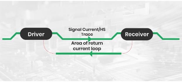
A reference plane in a PCB acts as a stable voltage plane, typically a solid layer of copper, providing an essential grounding path for high-speed signals. When used alongside signal traces, reference planes are pivotal in shielding traces against electromagnetic interference (EMI).
Reference planes are crucially important in designs with differential pairs, which are used for high-speed interfaces like PCI-Express and Serial ATA. Signal pairs are plus-and-minus combinations of two signals that need a certain level of reference plane to preserve signal quality, limit noise, and improve transmission efficacy.
Problems Encountered in High-speed PCB Design
With the increase in demand for the integrity of high-speed PCB signals, designers of PCBs tend to have a growing list of problems to solve:
- Complexity in Distribution of Power: Modern parts with multiple voltage levels have created cutouts in reference planes.
- Impedance Changes: Changes in trace thickness, spacing of differential pairs, or nonuniform reference planes can result in severe signal reflections and information loss.
- Electromagnetic Interference (EMI): Cuts in the reference plane can create undesired signals that contribute to a signal’s degradation.
- Crosstalk: The coupling of adjacent traces can result in the loss of a specified signal.
PCB Reference Plane Design Guidelines
The following goals can help structure the PCB reference plane design for efficient high-speed signal transmission:
1. Solid, Uniform Planes
Do not allow cuts or gaps in the reference plane. Breaks in planes lead to signal distortion due to unstable impedance paths.
2. Efficient Use of Ground Layer
Ground planes should be placed next to high-speed signal layers in addition to signal layer loops. This configuration helps improve the quality of the signals while minimizing signal loops.
3. Differential Pair Routing Control
Traces should maintain equal spacing from the reference plane to help control differential pair routing. The above setup enhances impedance control and allows the reduction of signal suffrage.
4. Via Reduction
Reducing vias helps preserve high-speed PCB signal integrity, as each via discontinuity can have a distinct impact on high-speed signals. Where required, place them away from return paths to help maintain signal integrity.
5. Guard Important Signals From Interference
For traces with high EMI and crosstalk, it would be best to use shielding or guard traces to reduce interference in environments where noise is rampant.
6. Confirm The Results of The Impedance Computation
Employ simulation software for the network to compute, in addition to confirming the results pertaining to trace impedances and differential impedance, which is usually 100 ohms in high-speed situations.
Impact of Slits on Signal Transmission
Due to the advancement of multi-power designs, cuts in the reference plane are often necessary. Understanding the effects of these cuts on signal propagation is equally important in order to reduce negative consequences.
Experimental Findings
One of the effects noted was that the insertion of a 5mm slit in a microstrip reference plane resulted in a differential increase of approximately 6 ohms. The Sdd21 measures showed a significant recession of propagation signals when the common mode impedance (Zcom) was lower.
Within this study, the authors presented mathematical models to demonstrate how the effect of the slits. This information can assist designers when devising a plan to alter the design that seeks to enhance the transmission characteristics.
Primary Measurement Methods of High-Speed PCB Signals
For optimal Testing and Measurement, a high-end standard is followed by PCB circuit board fabricators. Some of these techniques include:
1. Time Domain Reflectometry (TDR)
TDR gives Time Domain Reflectometry the ability to reflect pulses from a line communication and perform analysis of transmission. To facilitate the interpretation of problem areas like slits in reference planes.
2. Transmission and Crosstalk Analysis
Broadband network analyzers do not measure transmission losses or crosstalk. This information is crucial in helping designers measure how different facets of the signal design affect its integrity.
3. S- Parameter Analysis
Static S-Parameter synthesis allows the Designer to perform S-Parameter simulation and pristine quality verification of Signal Transmission. This may also include suggesting alternatives to the existing assembly or routing novel transmission paths.
Practical Approaches to High-Speed Signal Integrity
The techniques to tackle PCB reference plane design disruption problems:
1. Stitching Capacitors
The introduction of stitching capacitors can solve the placement of slits or gaps. These slits and the stitching capacitors provide a routing low impedance during high frequencies.
2. Differential Pair Shielding
Employ shielding where routing of differential pairs across a slit is considered.
3. Simulation and Modeling
Use prediction tools to diagnose, anticipate, and rectify shortcomings before it is too late. Due to the introduction of simulation technologies, designers now have the ability to evaluate how modifications will affect the overall high-speed PCB signal integrity prior to the physical production stage.
4. Design Rule Checks (DRC)
Ensure that reference planes are relevant and consistent throughout the entire structure via thorough DRCs with special emphasis on high-speed signal design guidelines as supporting criteria.
Emerging Trends in High-Speed PCB Design
Newer devices and higher data rates must match technology’s evolution, requiring a more refined PCB design style. Advanced materials like low-loss laminates are rapidly emerging in the market for high-speed designs. Furthermore, engineers are solving the complex challenges of high-speed PCB signal integrity with the help of powerful simulation tools and artificial intelligence-based design optimization.
PCB circuit board manufacturers need to be at the forefront of innovation to stay competitive and provide advanced technologies.
Conclusion
To integrate maximum permittable signal transmission speeds in PCB designs, reference plane techniques need to be modified strategically. Consistency in reference planes, optimal routing of differential pairs, and rigorous testing are some of the steps that PCB circuit board manufacturers need to take to design for the modern high-speed world.
By carefully planning and following best practices, PCB circuit board manufacturers can overcome design challenges while achieving high-speed PCB signal integrity and effective performance in demanding environments.
Stay updated with such information at PCB Runners.