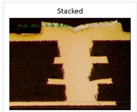
Stacked Vias: What Does It Mean?
Stacked vias are created by stacking numerous vias on top of one another. To ensure an electrical connection, each via would be drilled first, then metalized with a small annular ring at the top and bottom. Because the annular ring is frequently extremely thin—about.002 inches—very precise registration is required. Because stacked vias may be stacked on top of one another and take up less space on a circuit board than through-hole vias, they are more flexible and practical for efficient routing of high-density boards. The efficient use of the stacked vias allows for total flexibility in the layer connection. Additionally, it reduces its parasitic capacitance, which is frequently connected to vias. More steps are required throughout the PCB manufacturing process when using stacked vias to ensure a strong inter-via connection. Even at slightly higher prices, the increased routing flexibility often makes the difference between being able to route the design well and not being able to, which results in better design solutions. According to our engineering staff, using this layout strategy will become more and possibly even critical as component densities increase and the board’s surface area decreases.
What Advantages Do the Stacked Vias Offer?
Stacked vias are created by stacking numerous vias on top of one another. To ensure an electrical connection, each via is first drilled and then metalized while keeping a small annular ring at the top and bottom. Since the annular ring is frequently quite narrow—as thin as .002′′—very precise registration is required.
Less space
Additionally, since one via may be piled on top of the other, stacked vias take up less space on a circuit board than through-hole vias, increasing the possibility that the high-density board will become more flexible and useful.
Flexibility in layers of connectivity
The efficient use of the stacked vias allows for complete flexibility in layer connectivity. Additionally, it reduces its parasitic capacitance, which is frequently connected to vias. Further steps are required during the fabrication of PCBs with stacked vias in order to ensure a strong inter-via connection.
However, even at somewhat higher costs, greater routing flexibility often makes the difference between being able to route the design successfully and failing to do so, leading to better design solutions.
Improve density and size concerns
With today’s shrinking, high-signal transmission performance, and scalability in many applications, stacked vias are a way to further improve density and size concerns when creating printed circuit boards (PCBs), two very important factors.
When drilling requirements span multiple layers and blind vias have aspect ratios greater than 1:1, stacked vias may be the most reliable internal connection solution.
Better routing capabilities, lower parasitic capacitance
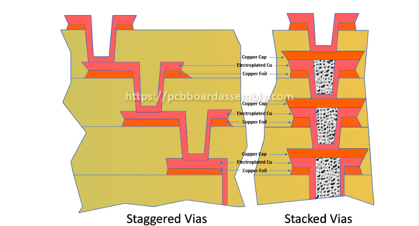
Also referred to as laminated buried and blind vias and stacked vias, many vias are formed together around a single center. Staggered vias are laminated vias that have distinct centers. Stackable vias not only increase density and save space, but they also provide better routing capabilities, lower parasitic capacitance, and greater flexibility for interior connections.
Challenges in manufacturing stacked via PCBs
The following issues should be taken seriously, even though it is challenging to identify the precise requirements that may result in failure:
Aspect Ratio
Reliability increases with smaller aspect ratios. Microvias (stacked vias) with an aspect ratio of 0.7, for example, have been shown to withstand accelerated life tests but microvias with an aspect ratio of 1 fail after a few thermal cycles.
Voiding
While voiding is associated with failure, its volume and form, as well as the stacked vias aspect ratio, have a more significant role. Consequently, it is not possible to say with certainty that voids always result in a higher failure rate.
Stacking versus scattering
The criteria used to compare the dependability of staggered versus stacked microvias are inconsistent. Generally speaking, designers try to stagger the other micro vias in the vertical interconnect by stacking no more than two microvias vertically.
Plates made of copper
The thickness of the plating at the butt joint causes failure, even when the copper wrap coating does not.
Arguments in Favor of Hiring an Expert in PCB Stacked via Design
Four Arguments in Favor of Hiring an Expert in PCB Stacked via Design and Layout Services
Numerous PCB manufacturing and assembly companies focus exclusively on particular tasks or provide third-party services to large PCB manufacturers. Nonetheless, the methodology of a seasoned provider of PCB design for stacked and layout services sets them apart. The following guidelines will assist you in realizing the advantages of collaborating with them.
1. Technical Competency:
A lot of PCB design concepts are unsuccessful and never result in functional prototypes. The manufacturer’s and product designer’s lack of sight is one of the main causes. You can get advice on concept generation, schematics, and prototype construction from a skilled PCB designer. Working with them will enable you to create layouts that fit your company’s needs.
2. Rectify Design Flaws:
Many design errors are introduced at the conceptualization stage, and if they are not fixed, they may result in operational inefficiencies at a later stage. Skilled PCB designers are frequently able to spot these defects and offer fixes to lessen the problems. Additionally, at various iteration stages, design defects may be introduced. The designers may be quick to spot these and provide you with an ideal solution.
3. Reduce Time, Efforts, and Costs:
There are a number of components or considerations that go into PCB design and layout, which could drive up expenses. By examining your design plans, the PCB design experts can frequently quickly determine the elements that may contribute to your expenditures. To increase efficiency, they could even advise you to simplify the designs or recommend replacing some parts. They might even assess what needs to be improved by comparing your schematics with the current boards.
4. Enhanced Time-to-Market Competencies:
In order to effectively meet the needs of their customers, the majority of firms today strive to increase their time-to-market capabilities. You may reduce the likelihood of product failure by building efficient, functioning prototypes more quickly with the assistance of a specialized PCB design and layout service. Therefore, you can be confident of the meticulous planning and efficient designing and manufacturing that follow if you collaborate with an expert PCB designer. You’ll notice a noticeable improvement in the speed of your production and prototyping.
Why Should You Hire a PCB Runner to Design Your Circuit Board?
PCB Runner is a proponent of doing things correctly the first time. Therefore, before we send your product, we ensure that there are no mistakes or omissions. Our customers benefit from this by saving money, time, and the hassle of constant adjustments and corrections.
A fully personalized PCB design and layout service is provided by PCB Runner. Additionally, we provide PCB assembly and prototyping services, enabling us to validate the design before committing to mass production.
Our Principal Area of Specialization and services related to stacked via pcb manufacturing
Our speciality is offering:
- Superior surface mount design for µBGA, BGA, PCIE, PCI, CPCI, and further applications
- Three designs: rigid, flex, and rigid-flex
- Controlling differential impedance
- High-velocity signal arrangement
- Ultra-low EMC/EMI design for magnetic resonance imaging
- Design of sensitive analogue circuit boards
- High-frequency layout and design of PCBs
- High voltage and high current architecture
- Plan for Construction
- Create with Manufacturing in Mind
- Expert paperwork for the fabrication
- Create with Testability in Mind
- PCB manufacture and assembly, as well as prototype
- Examining circuit boards
- Producing In-Circuit Testing Data
Manufacturing Stacked Vias
Compared to staggered vias, stacked vias require additional steps in the production process. As a result, it is more difficult. This is where several vias are stacked on top of each other. They connect multiple layers with low space usage. Each via is drilled and then plated prior to being stacked on top of one another. There are two narrow, annular rings available on the top and bottom.
The upper one indicates precise registration, while the lower one is used for electrical connections. The design consists of three separate acts:
- Filling copper holes
- Planarization
- Further imaging
- Copper filling with stacked vias
Every stacking via is filled with electroplated copper. It provides structural stability and ensures a dependable electrical connection. There may occasionally be flaws in the copper that has been deposited. The following difficulties are explained:
When copper is deposited incorrectly, vias might turn into voids. Such cavities inside the framework lead to localized stresses. As a result, the same reliability of stacked microvias can be compromised.
Poorer bonding occurs between the target pad beneath the microvia and its base when electroless low-grade copper is used.
Advanced techniques and materials used for stacked via fabrication
Copper filling
Electroplated copper is filled in stacked vias. This gives strong structural support along with providing solid electrical connections in pcb. Sometimes situation occurs when defects have been seen in electroplated copper for example :
- Inappropriate filling creates gaps in vias. This can result in the generation of localized stress in the structure of PCB. This can also affect the reliability of stacked microvias.
- Poor-graded copper has no proper electrolytic properties resulting in inferior bonding of the base of microvia with the target pad.
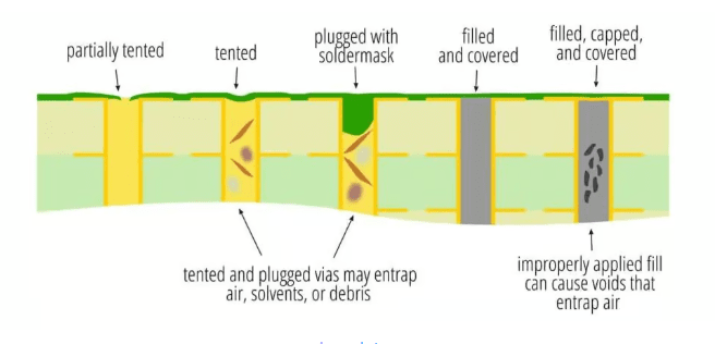
Microvia Filling Procedure
The micro via that is stacked needs to be filled and either buried or have a copper cover placed on it. The fact that the HDI PCB Manufacturer creates an electrical channel that incorporates the copper cap in the structure that the micro via is layered onto is one of the issues with stacked via. Accordingly, until the PCB manufacturer stacks another structure on top of the copper cap, it is not a component of the circuit.
Microvias and buried vias in stacked structures need to have a fill layer in addition to their caps in order for the copper cap to develop.
To ensure good electrical contact with the plated copper wrap and to reduce the copper thickness, they typically include a planarization step. Currently, three fill types are used in the production of HDI PCBs. One possible fill material is electrolytic copper plating, often known as “a-stage” fill material or the dielectric system’s liquid. or an epoxy fill by a third party. The barrel crack failures are prevented by the solid copper of the entire micro via (or, in rare cases, the hidden one) and the good electrolytic copper plating. Because the “a-stage” fill precisely matches the underlying dielectric material’s glass transition temperature (Tg) and coefficient of thermal expansion (CTE), it is considered to be good.
The third-party fill does not have the same Tg and CTE as the base material, regardless of whether it is conductive or not. Every fill kind has benefits and drawbacks of its own.
Planarization Method
During the HDI PCB fabrication process called planarization, the fill and some of the wrap-related copper are removed from the microvia’s knee or buried via to thin the copper layer between layers and create a strong bond between the copper wrap and the electroplated cap. An open circuit could result from a conductivity issue between the wrap and the cap if the planarization is not aggressive enough. An excessively aggressive planarization can result in an excessively thin wrap, which can cause damage from knee cracks. The fact that the third-party fillers typically have a different Tg and CTE than the epoxy of the base dielectric layers is an issue. These variations may cause issues when these are utilized to fill buried vias or microvias.
Standards for Manufacturing and Quality Control
When choosing a High-Density Interconnect (HDI) stacked vias PCB provider, quality control and adherence to production standards are essential factors to consider. Let’s examine why taking these factors into account is essential to guaranteeing the dependability and functionality of your electronic devices.
Consistency in Quality:
Throughout the manufacturing process, a trustworthy stacked via based PCB supplier upholds strict quality control procedures. By delivering PCBs that meet or surpass your standards, this consistency in quality lowers the possibility of errors and guarantees dependability in your final products.
Standards and Certifications:
Seek vendors with certifications such as ISO 9001, a widely accepted standard for quality control systems. These accreditations show a dedication to excellence and a follow-through with accepted industry norms.
Extensive Testing:
Find out how the provider conducts testing. Before the PCBs are supplied to you, a trustworthy supplier should perform a battery of tests, such as electrical, impedance control, and reliability testing, to find and fix any problems.
Material Traceability:
Materials must be traceable, particularly in sectors where regulations are stringent. For compliance and troubleshooting purposes, knowing the origin and history of the materials used in your PCBs can be quite important.
Failure Analysis:
A reliable system for failure analysis has to be in place at a provider that prioritizes quality. If there are any flaws or problems, they ought to be able to find the source right away and put preventative measures in place to stop it from happening again.
Continuous improvement culture
Selecting a supplier who upholds a continuous improvement culture is important.
These vendors guarantee that your PCBs take advantage of the newest breakthroughs in the market by continuously improving their processes and keeping up with industry developments.
Paperwork for Quality Control:
Verify that the supplier includes thorough paperwork for quality control with every shipment. These records, which provide transparency and assurance about the caliber of your PCBs, ought to include a detailed account of the testing and inspection outcomes.
Integration of Customer Feedback:
Reputable vendors actively seek out and consider input from their clients. They are able to meet particular project requirements and consistently improve the quality of their services because of their customer-centric approach.
Industries and products that benefit from multilayer stacked via technology
In fact, because of their benefits, multilayer PCBs are ideal for a wide range of sectors and uses. Below are a few particular applications for multilayer printed circuit boards:
1. Consumer Electronics:
A wide range of consumer electronics, including tablets, smartwatches, smartphones, and other portable gadgets, use multilayer printed circuit boards (PCBs) having stacked vias. The development of advanced features and multitasking capabilities in these devices is made possible by the high functionality and compact size of multilayer PCBs.
2. Telecommunication Equipment:
Because of their strength and resilience to harsh weather, multilayer printed circuit boards (PCBs)having stacked vias are the standard in the telecom sector. They are found in routers, base stations, mobile devices, and other telecom hardware.
3. Industrial Equipment:
Industrial controls and machinery are a good fit for multilayer printed circuit boards. They are appropriate for severe industrial settings where equipment may be subjected to rough handling or extreme circumstances because of their longevity and dependability.
4. Medical Equipment:
Multilayer printed circuit boards (PCBs) stacked via technology are essential components of medical equipment, such as imaging, monitoring, and therapy devices as well as diagnostic tools. Advanced medical technology development is aided by the mobility and functionality that multilayer printed circuit boards (PCBs) offer.
5. Military & Defense Equipment:
Compact designs and high-speed circuits are essential for the equipment used by the military sector. Our Stacked via PCB are perfect for military and defence applications because they allow for the integration of various functionalities while retaining mobility and reliability.
6. Automobile sector:
Onboard computers, engine control units, sensors, and other electronic components are among the many applications for Stacked via PCB in the car sector. Their tiny form size, superior performance, and resilience to heat make them ideal for the demanding needs of automotive applications.
7. Aerospace sector:
High-performance, lightweight, and small electronics are required for the aerospace sector. In the aerospace industry, multilayer printed circuit boards are used in satellite technology, navigation equipment, communication systems, and cockpit computers.
8. Computer electronics:
High-performance computing systems, servers, laptops, and desktop computers all make heavy use of Stacked via PCB. They offer the dependability, performance, and compactness needed for computer motherboards and other parts.
Read More: Solving Common Issues in Edge Plating PCBs Tips and Tricks
Pcb Runner Quality Control Commitment
Strict Quality Control
At PCB Runner, we recognize the value that PCB functionality and quality have for our clients. For this reason, we incorporate quality-oriented concepts throughout every stage of the assembly and production of PCBs. We are still dedicated to conducting all PCB-related activity in accordance with recognized worldwide quality standards.
We ensure that every one of our assembled and bare PCBs meets or surpasses the exact specifications provided by our customers. Our reputation for excellent quality, timely delivery, and competitive pricing is attested to by our clientele.
Our products are guaranteed to be of the highest quality and dependability thanks to our strict manufacturing procedures. International standards like ISO9001 are met by us, and we are eligible for IPC Classes 2, 3, and 3A.
Why Opt for PCB Runner?
There are various benefits to selecting PCB Runner as your printed circuit board maker. We provide quick turnaround times on all kinds of high-quality PCB services. We put every PCB through quality and reliability testing.
Kindly visit our website to acquire an estimate for any bespoke circuit board you may need.
Certifications and Registrations for PCB Runners
ACCREDITATIONS
We withhold a number of PCB certifications as a symbol of our dedication to the quality management system, demonstrating our steadfast commitment to upholding standards of quality.
Use the icons below to browse through our official certifications.
The 2015 ISO 9001 standard
ISO 14001:2015
ISO 13485:2016
Our engineers are all certified IPC A-610 personnel. Please get in touch with us if you would like more information.
The PCB Runner Advantage
For the production and assembly of fully functional printed circuit boards, PCB Runner is the recommended option. The diversity and adaptability of the solutions we provide are preferred by our clients. We provide every kind of printed circuit board you need, ranging from single-layer to multi-layer, rigid boards, rigid-flex boards, and HDI boards. No matter the quantity of your purchase, we can handle boards of any form or size that you require.
The fact that PCB Runner has specialists for every step of PCB assembly and manufacturing is by far our greatest asset. We provide PCB fabrication and assembly services that are full turnkey, partial turnkey, and full feature. To put it briefly, we provide a comprehensive end-to-end solution for your projects. From design and manufacturing to assembly, testing, packing, and shipping, our professionals will be at your side every step of the way.
You will quickly see the benefits of working with PCB Runner for your PCB fabrication and assembly since they are a one-stop shop, saving you the trouble of contacting multiple businesses to finish your project.
Our Proficiency
- PCB Panels
- Layer Stack up, Blind, and Buried Via’s
- Lead-Free
- Soldering Through Laser
- Micro Via
- Via in Pad
Full-featured PCB Manufacturing and Assembly Capabilities are offered by PCB Runner
- Stiff PCBs
- Flexible PCBs
- PCBs that are rigid-flexible
- PCBs using High-Density Interconnect (HDI)
- PCBs with many layers
Base Materials for PCBs
What we can offer you is:
- PCBs at High Temperatures
- PCBs that comply with RoHS regulations
- PCBs with High-Frequency RF
- Fast Digital PCBs
- Prototype PCB Assembly, PCB Services, and PCB Assembly
- Sources for Components: Low Volume, High Volume, Partial Turnkey, and Full Turnkey PCB Assembly
PCB Runner offers custom design manufacturing for all industries along with critical stacked Via’s / Elic design requirements. Please do submit your schematics & BOM files to our email at sales@pcbrunner.com or engineering@pcbrunner.com

