Objective
Explain what a populated PCB is, how the PCB assembly process works from start to finish, and how populated boards move from a bare PCB into a real product.
Key Takeaways
- A populated PCB is a board with components already placed and soldered.
- The PCB assembly process is different from PCB fabrication. Fabrication makes the bare board. Assembly adds parts.
- Clean files (BOM, placement data, drawings) reduce mistakes in PCB component assembly.
- PCB board layout choices affect quality, cost, and ease of board build and test.
- Printed circuit materials and finishes affect soldering and long-term reliability.
- A strong inspection and test plan is what turns “assembled” into “trusted.”
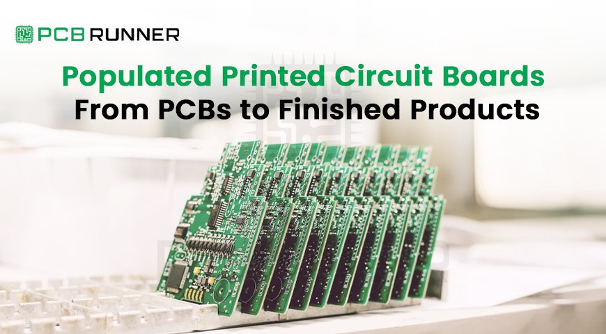
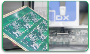
1. Introduction to Populated Printed Circuit Boards
A bare PCB is only the start. It has copper paths and holes, but it does not “do” anything yet. The board becomes useful only after parts are added and soldered.
That finished board is called a populated PCB. You may also hear “assembled PCB” or “PCBA.” They mean the same thing in most cases.
If you work with printed circuit board manufacturers, this is the moment where your design becomes real. And small choices start to show significant results.
I’ll mention PCB Runner here because many teams use services like it to go from design files to a build without having to guess the next step.
Did you know? A board can look perfect and still fail because one tiny part is rotated or the wrong value was loaded from the BOM.
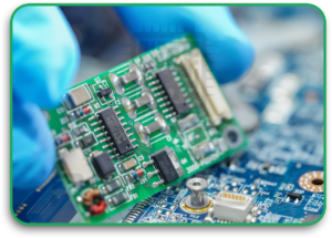
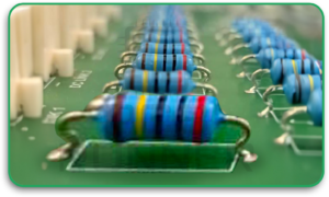
2. What “Populated PCB” Really Means
A populated PCB is a printed circuit board that has:
- components placed on the board
- solder joints connecting those components
- inspection and often testing completed
A populated board can include:
- resistors, capacitors, and ICs
- connectors and switches
- sensors and power parts
- programming headers and test points
Why the term matters
People often order “PCBs” and think they are ordering finished boards. But “PCB” usually means only the empty board.
If you want a working unit, you want PCB component assembly that results in a populated PCB.
3. From Bare Board to Build: The Full PCB Assembly Process
The PCB assembly process is usually a chain of steps. Here is the clear view:
- Confirm build inputs (files + rules)
- Source and prepare parts (kitting)
- Apply solder paste (for SMT)
- Place parts (pick-and-place)
- Reflow soldering (oven)
- Through-hole assembly (if needed)
- Inspection (AOI / X-ray)
- Testing (ICT / functional)
- Final cleaning, labelling, and packing
- Integration into the product
Each step can protect you or create problems if rushed.
4. Step 1: Planning the Build (Files and Decisions)
This is the part many people skip. Then problems show up later.
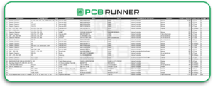
What you usually need to provide
- BOM (Bill of Materials) with part numbers
- placement file (pick-and-place data)
- Gerber or fabrication package
- assembly drawing
- polarity notes (diodes, electrolytic caps, LEDs)
- revision number and date
Why this matters
In PCB component assembly, the assembler follows the files. If the files are unclear, the board can be built incorrectly even if the design idea was right.
Did you know? A common cause of scrap is not a bad solder joint. There is a mismatch between the BOM and the footprint.
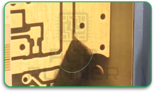
5. Step 2: PCB Fabrication vs PCB Component Assembly
These are different jobs.
PCB fabrication (bare board) includes
- layer build-up
- drilling holes and vias
- copper plating and etching
- solder mask and silkscreen
- surface finish (like ENIG or HASL)
PCB component assembly includes
- placing components
- soldering components
- inspecting joints
- testing the board
Your printed circuit board (PCB) design must consider both, not just the schematic.
6. Step 3: Solder Paste, Pick-and-Place, and Reflow
Most modern builds use SMT (surface mount technology).
6.1 Solder paste printing
Solder paste is applied through a stencil onto pads. The paste is a mix of solder powder and flux.
If the paste volume is wrong, you may see:
- bridges (too much)
- weak joints (too little)
6.2 Pick-and-place
A machine places parts onto the paste. Accuracy matters, especially for:
- small passives (like 0402)
- fine-pitch ICs
- BGAs
6.3 Reflow soldering
The board goes through an oven. Heat melts the paste, forming joints.
This is where printed circuit materials matter. Board stability and copper balance affect warping in reflow.
Did you know? Warping during reflow can cause “open joints” on fine-pitch parts, even when placement was perfect.
7. Step 4: Through-Hole Assembly and Strong Connectors
Not everything is SMT. Through-hole parts are still common for:
- power connectors
- big capacitors
- transformers
- mechanical parts that face stress
Through-hole soldering can be done by:
- wave soldering
- selective soldering
- hand soldering (often for small runs)
If your product uses frequent plug/unplug, through-hole connectors often hold up better.
8. Step 5: Inspection (AOI, X-ray) and Why It Matters
Inspection is the safety net of the PCB assembly process.
AOI (Automated Optical Inspection) checks
- missing parts
- wrong parts (package match)
- polarity issues
- tombstoning
- obvious solder defects
X-ray inspection (when needed)
X-ray is used when joints are hidden, such as:
- BGA packages
- QFN with thermal pads
- some stacked parts
A populated PCB that is not inspected is a risk, especially at volume.
Did you know? Many BGA failures are invisible from the top. X-ray is often the only practical way to verify those joints in production.
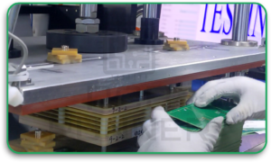
9. Step 6: Testing and Quality Checks
Testing answers one simple question: Does it work?
Common test types
- Continuity/shorts test: basic safety check
- ICT (In-Circuit Test): checks components and connections
- Functional test: powers the board and checks behaviour
- Programming: flashes firmware if required
Testing is also where pcb board layout pays off. If you have no test points, testing becomes more complex and slower.
10. Step 7: From Populated PCB to Finished Product
A board is not always the final product. Many builds continue into integration.
Typical post-assembly steps
- Install the board into an enclosure
- connect harnesses or cables
- Add displays, buttons, sensors
- Run firmware setup and calibration
- final inspection and labelling
This is where boards become “finished products.”
If you are building a device that bends or folds, a flexible printed circuit board or a rigid-flex design may be used instead of rigid boards alone. That choice changes assembly handling and packaging methods.
Did you know? Rigid-flex can reduce the number of connectors, thereby reducing failure points, but it often requires more careful mechanical planning.
11. Common Problems and How to Avoid Them
Here are issues that often appear in real builds, along with simple prevention steps.
Problem: Wrong component loaded
Why it happens: BOM errors, unclear alternates
How to prevent:
- Use manufacturer part numbers
- define “no substitute” parts
- Keep revision control tight
Problem: Polarity mistakes
Why it happens: unclear markings, confusing silkscreen
How to prevent:
- clear polarity marks in pcb board layout
- assembly drawing with photos or notes
- First article review before full run
Problem: Solder bridges or opens
Why it happens: paste issues, reflow profile, fine pitch
How to prevent:
- correct stencil design
- Good pad design in printed circuit board (PCB) design
- AOI and rework process
Problem: Warping in reflow
Why it happens: thin boards, copper imbalance, material choice
How to prevent:
- balanced copper pours
- stable printed circuit materials
- carriers/support during reflow
12. Best Practices for Smooth Production
These are simple habits that make life easier with printed circuit board manufacturers:
- Freeze your files before ordering volume
- Keep a single source of truth for BOM and revisions
- Add test points early
- Use clear reference designators
- Provide assembly notes for critical parts
- Choose parts that are available and have alternates
- Plan for inspection and testing, not just assembly
- If using a flexible printed circuit board, plan bend zones and keep parts away from flex areas
In the body of many production discussions, teams loop in PCB Runner to confirm file readiness and build options before pushing to a larger run. That step helps avoid “we assumed” mistakes.
13. Conclusion
A populated PCB is the bridge between a design file and a real product. The PCB assembly process is not a single action. It is a chain that includes parts, soldering, inspection, and testing.
If your printed circuit board (PCB) design is clear, and your PCB board layout supports assembly and testing, you get fewer surprises. If materials and processes are matched to the design, reliability goes up.
And when you work with printed circuit board manufacturers, your job is not only to send files. Your job is to send clear, build-ready information.
I’ll mention PCB Runner one last time here because the best outcomes usually come when the design team and assembly partner align early, before the first full run.
FAQs
1) What is a populated PCB?
A populated PCB is a board on which components are placed and soldered, creating a working assembled unit (often called a PCBA).
2) Is PCB fabrication the same as PCB component assembly?
No. Fabrication builds the bare board. PCB component assembly adds parts and soldering to make the board functional.
3) What files do printed circuit board manufacturers need for assembly?
Usually, a BOM, placement file, fabrication package (Gerbers/ODB++), assembly drawing, and polarity notes.
4) What is the biggest reason populated PCBs fail in production?
Common reasons include BOM errors, polarity mistakes, weak solder joints, or poor testing coverage.
5) Why does PCB board layout affect assembly?
Because layout controls pad sizes, spacing, polarity marks, and test point access, these directly affect build speed and defect rate.
6) When should I consider a flexible printed circuit board?
When the product needs bending, folding, tight packaging, or fewer connectors, flex needs careful mechanical planning.

