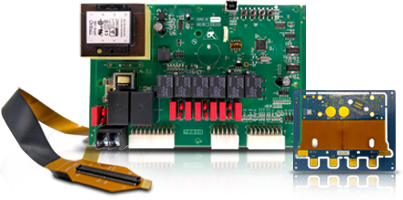
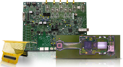
PCBs are incorporated in nearly all electronic devices, thereby necessitating their precise design and reliable functioning. Specialized computers, smartphones, automotive gadgets, and aerospace industry features all need computer boards, and consumers require their performance to be dependable and of high quality. This brings about the major role of the PCB Manufacturing process and its manufacturers. PCBs Trip through a thorough step-by-step process to try to guarantee that the final product of the board meets the complications required.
Knowing PCB board manufacturing techniques is crucial to experts, designers, and engineers, and in this situation, we try to shed light on the most relevant processes needed to transform raw materials into readily available products through manufacturing techniques, processes, and advanced engineering.
Your best bet for ready-to-use PCBs is PCB Runners, who are willing to assist and offer appropriate pcbs-sales for your specific needs.
Understanding the PCB Manufacturing Process
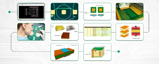
The entire manufacturing PCB process needs special attention due to its multistep nature; each step independently contributes to the durability and functionality, with each requiring focus. The typical order of operations in PCB production includes:
- Design and Prototyping
- Material Selection
- Layer Preparation
- Inner Layer Imaging and Etching
- Laminating
- Dry Film Application and Copper Plating
- Drilling and Plating
- Solder Mask Application
- Silkscreen Printing
- Surface Finishing
- Quality Inspection and Testing.
Step 1: Design and Prototyping.
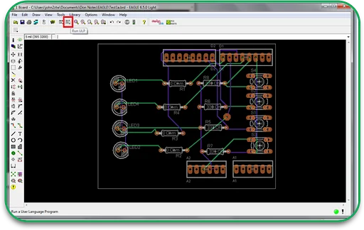
Designing a schematic as a first step in the PCB manufacturing process is one of the vital processes and must be done thoroughly. Using computer-aided design (CAD), composite software used in the industry enables engineers to design circuits in PCB templates; they set the position of holes and components and decide on what routes will be used for the traces.
Once the design is complete, a prototype is made to test how it works before mass production. Prototyping is essential for checking if the design can be manufactured and identifying any issues.
Step 2: Material Selection
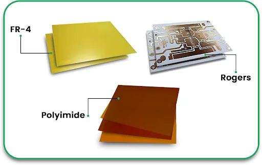
Durability, as well as thermal resistance and conductivity, depend on the PCB material choice. Listed below are some of the materials used by PCB circuit board manufacturers:
FR4 (Fiberglass Epoxy) – Standard material for general-purpose PCBs.
Polyimide – Used for flexible and high-temperature applications.
Metal Core (Aluminum or Copper) – Ideal for power electronics and LED boards.
High-Frequency Laminates – Required for RF and microwave circuits.
Step 3: Layer Preparation
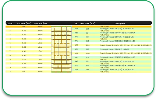
For multilayer PCBs, manufacturers start by fabricating individual layers. Each layer consists of:
Copper foil – Conductive paths for electrical signals.
Prepreg – Insulating layers for electrical separation.
Substrate – The structural base of the PCB.
Step 4: Inner Layer Imaging and Etching
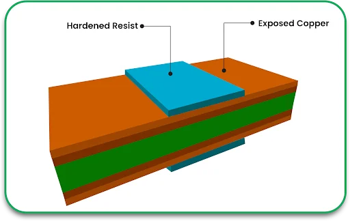
Manufacturers employ photoresist imaging to create the circuitry of the PCB.
- Stick a photosensitive photoresist film on the copper layer.
- Define the circuit pattern by exposing a mask with UV light through a lens.
- Get rid of unwanted copper after developing it, and retain the traces for the circuits.
For multilayer PCBs, this approach is used for each layer until they are stacked together, and the process is repeated.
Step 5: Lamination
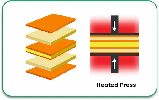
In this step, each layer is aligned and laminated under heat and pressure to create a solid PCB stack. This bonding procedure guarantees electrical and mechanical integrity failure.
Step 6: Drilling and Plating
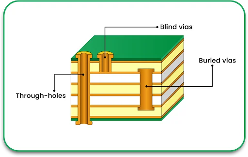
After lamination is completed, holes are drilled to enable electrical connections between the layers. Different hole types are available:
Through-holes: Pass throughout the board.
Blind vias: Connect outer layers with inner layers.
Buried vias: Connect only internal layers.
After being drilled, the holes are plated with copper to form conductive paths. The thickness of the plating has an impact on the electrical performance and reliability of the unit.
Step 7: Solder Mask Application
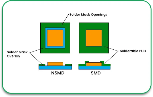
A solder mask layer is put on to shield the copper traces from oxidation and short circuit damage. The solder mask:
- Prevents the solder from bridging.
- Enhances durability.
- Improves the overall appearance of a PCB.
Commonly used solder mask colors include green, red, blue, and black.
Step 8: Silkscreen Printing
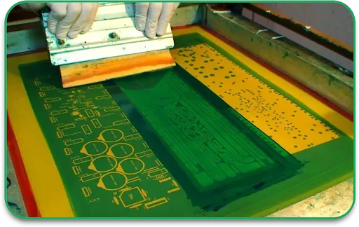
One more step needs to be completed before the PCB is finished, and that is to use silkscreen printing to put the components’ names, polarity, and the company that made the PCB for identification purposes so that engineers can quickly troubleshoot issues during assembly.
Step 9: Surface Finishing
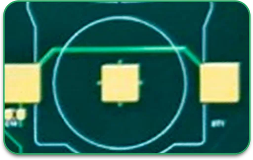
In fulfilling the requirements of solderability and protection, PCB board fabricators apply surface treatments on copper-exposed pads. These treatments serve to preserve as well as enhance solderability. Some types of finishes for PCBs are:
HASL: Hot Air Solder Leveling. It is the least expensive and one of the most frequently used.
ENIG: Electroless Nickel Immersion Gold Best for gold-plated applications for vital and security equipment.
OSP: Organic Solderability Preservative Value friendly and used for fine-pitch lead components.
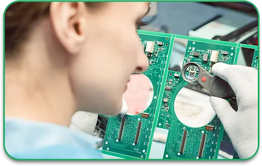
Step 10: Quality Inspection and Testing
In-house QC performs final checks:
AOI: Automated Optical Inspection Performs automated scanning for errors.
X-Ray Inspection. Exposes hidden solder joints to check for defects.
Electrical Testing. Make sure the circuits are all working properly.
Functional Testing. Put the system through actual operating conditions for testing.
Why Choosing the Right PCB Manufacturer Matters
Collaborating with seasoned PC board manufacturers offers guaranteed:
Consistent Reliability: Best equipment alongside stringent quality control will deliver high-quality PCBs.
Turnaround Time on Delivery: Batches of circuit boards get produced at once and then packaged in a single step.
Flexibility In Design: Those who wish to have their circuit boards printed differently will have their request accommodated.
Cost Efficiency: A savings-friendly workflow in PCB manufacturing.
Call PCB Runners now for quality PCBs and enjoy competitive rates. We offer PCB sales and cheap expert step-by-step PCB manufacturing services!
Conclusion
This is why knowing how the process of designing and building the PCB board works is crucial. These steps help refine strategies engineers and designers use in crafting devisable models geared for production. However, precision planning, as well as selection of materials, and elaborate testing, are needed for reliability.
Contact skilled manufacturers to guarantee precision PCBs that conform to industry standards of quality, reliability, and performance.
Are you Looking for a Trustworthy PCB Manufacturer?
With over 10 years of experience in the PCB business, trust PCB Runners to customize your order, providing expert solutions in the pc board manufacturing process. Get in touch today for affordable, tailored, high-quality PCB sales!
FAQs
1. Why are PCB manufacturing steps essential?
Following the workflow guarantees that every circuit board is functional and meets the minimum requirements of industry standards.
2. What is a PCB made of?
Materials such as FR4, Polyimide, Metal Core, and High-Frequency Laminates are frequently used depending upon the application.
3. What techniques do PC board manufacturers use to check PCBs for defects?
Inspection and testing are primarily done using Automated Optical Inspection (AOI), X-ray inspection, and electrical testing.
4. What are the common PCB surface finishes?
Some of the most frequently used finishes are HASL, ENIG, OSP, and Immersion Silver.
5. How much time does it take to manufacture a PCB?
The time taken varies with the intricacy involved, however, standard production is usually 5-15 days.

