PCBs are part and parcel of modern electronics and technology. With the aid of technology, Printed Circuit Board designs are more complex than before and often have multiple layers that are meant to provide better component performance with higher density. Multi-layered boards would not be functional without Vias. Vias provide the electrical interconnection of the layers of a PCB, allowing the signals and power to move across the board without any issues. While aiding in higher-level functions, if not appropriately designed, vias might create defects of weakness, poor solderability, and other reliability issues on the board. An understanding of various via types and their best placement creates robust and efficient PCB Design.
Different Types of Vias and Their Function
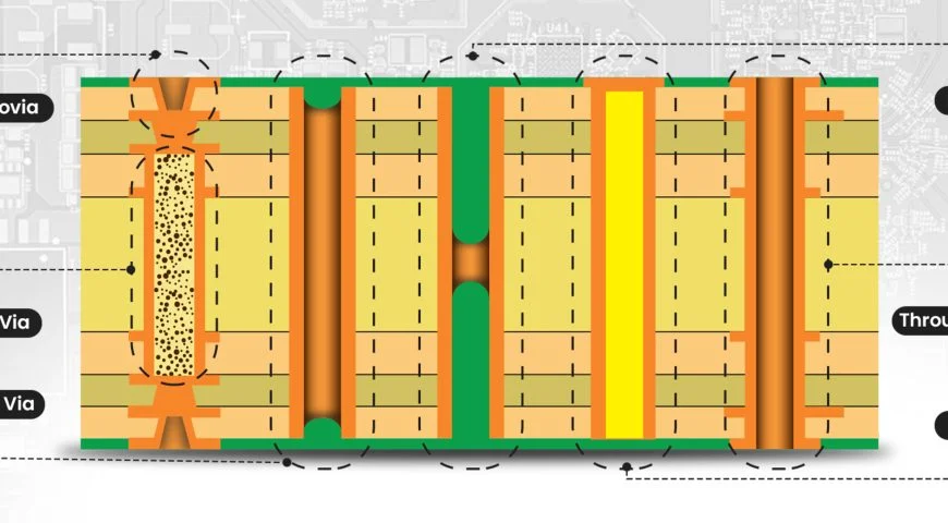
A via is a hole drilled into a PCB, plated with copper to form a conductive barrel that connects traces between different layers of the board. Depending on the method used to implement a via, it can have different uses on the PCB. There are three main types of vias used in PCB fabrication: through-hole vias, buried vias, and blind vias.
Through-Hole Vias
The most common of all via types is the through-hole via. It runs from the top layer of the PCB to the bottom, and the connection can be between any type of layer of PCB. Based on the design’s needs, the holes can be plated or non-lead through holes. As simple as the manufacturing process is, the holes are hefty in size and can cause issues if much of the available space is already limited.
Buried Vias
Solely associated with the inner layers of a multilayer printed circuit board, a buried via is concealed, which means it does not stretch to the top or bottom layers, therefore making it impossible to see from the outside of the PCB. For PCB designs that are high-density, these types of vias can help lessen surface space and make more compact surfaces. However, when compared to standard through-hole vias, they are more costly due to needing more intricate fabrication processes.
Blind Vias
Blind vias are a type of visa that starts from the outermost layer of the PCB, either the top or bottom layer and extends partially into an inner layer but does not extend fully through the board. They come in handy for designs that need high-density routing but need to save space on the outer layers. These are mostly used in high-speed compact PCBs where signal interference must be minimized.
The Role of Blind and Buried Vias in Modern PCB Design
Innovative designs for PCBs for applications such as telecommunications, medical devices, and automotive electronics makes use of blind and buried via because they can result in more compact yet reliable designs and improve performance. The benefits include:
- Increase in Routing Density: They allow the use of more compact space on the PCB, reducing the total size of the board.
- Enhanced Integrity of the Signal: Buried vias help increase signal quality for high-speed circuits by decreasing trace lengths.
- Greater Reliability: The overall robustness of the PCB is improved due to blind and buried vias, which reduce the number of layers exposed to environmental stress and increase durability.
In Perspective of Geometry of Vias
The dimension of a via is one of the most vital considerations in the design of the PCB. While larger vias can provide better mechanical support and more substantial conductivity, they also occupy more area, thus increasing the complexity of routing traces. On the other hand, smaller vias take up less space but are weaker, particularly when it comes to higher loads.
Drilling accuracy guidelines for adequate mechanical strength hardware to drill holes for the visa should not be narrower than 20 mils.
7 mil resolution annular rings should be the minimum value for traces annular rings for suitable attachment to the traces and walls of your vias is to traces.
The ratio of the via depth to its diameter aspect ratio (the ratio of the via depth to its diameter) is not to be more than 6 to 1 (or 6:1) because of subsequent reliability problems.
Peripheral Activities Met with Mounting Hole Design
The physical characteristics of the materials making up the components or parts of the boards will dictate the behaviour of most of the other physical attributes that will be active while the VC operates. The board materials expand as the components heat up and shrink when cooled down. Inevitably, stress will be applied to the via, causing it to crack and leading to electrical failures.
Ways to lessen the impact of thermal stress: use low-stress matched CTE materials for the vias.
To improve mechanical strength, increase the thickness of the copper plating in The Buried Vias, which will absorb excess mechanical stress.
Placing holes for the via away Reduces the amount of thermal cycling created by the board.
Avoiding Solder Wicking in Vias
Solder pads that are too close to vias can result in solder wicking, which happens when molten solder flows into the via during the reflow of soldering, causing the pad to have insufficient solder. Solely relying on the pad’s solder can lead to exposed poor solder joints that would lead to component failure.
Ways of Minimizing Solder Wicking
- Solder Mask Barrier: To prevent the solder from being drawn into the via, a solder mask can be strategically placed between the pad and the via.
- Tented Via: If the via is covered with a solder mask, it completely seals the via, thus preventing the solder from flowing through.
- Filled Via: When the via is filled with either non-conductive or conductive material and then covered with a tent, it provides a solid barrier against solder wicking and contamination.
Methods of Improving The Reliability of The PCB Vias
Adoption of modern approaches by fabricators is to increase the reliability of Vias in PCB designs, for instance, by:
- Via-in-Pad Design: It improves routing by placing the vias under a surface-mounted component. It also reduces trace length, thus improving overall performance.
- Back-Drilling: Commonly used in high-frequency applications, this method improves performance by removing unwanted stubs that reflect signals.
- Laser-Drilled Microvias: Most prevalent in HDI PCBs, these small interconnect vias are reliable and improve routing while necessitating fewer layers.
Choosing the Best PCB Manufacturer for Via Design
You must select a reputable PCB manufacturing company if your designs contain vias. Blind and buried vias are accurately produced by experienced PCB circuit board manufacturers using modern fabrication methods. Ensure that the PCB fabrication services you consider provide:
- Highly accurate drilling services
- Stronger plating for enhanced via strength
- Automated optical inspection (AOI) and X-ray analysis as quality control processes
Conclusion
PCBs cannot function accurately or reliably without vias. Regardless of using through-hole, blind, or buried vias, robust and effective planning, as well as design methodologies, are important to obtain high-performing and durable boards. Impacts of via size, placement, thermal matters, and solder wicking are critical to better PCB designs. By working with experienced PC board manufacturers and following best practices, the reliability, longevity, and effective performance of PCBs can be increased to withstand gruelling applications. Finally, putting effort in the right places via design results in compact and efficient electronic circuits that comply with industry standards.

