It is clear that the electronics sector is growing quickly, and sustainability is becoming an essential factor throughout every stage of production. Traditional custom printed circuit boards rely mainly on copper as the primary conductive material, along with other metals used in finishes and specialty inks. While they’re effective, these products leave a substantial environmental footprint due to the energy-intensive process chemicals, as well as their limited recyclability.
Carbon ink is emerging as a greener alternative in PCB manufacture, offering lower environmental impact while delivering reliable electrical performance for suitable applications. For designers and engineers who work on PCB manufacture. Understanding carbon ink is essential for adopting eco-friendly PCB manufacturing processes in modern electronics.
This article will explain the meaning of carbon ink, what it is, how it works, the benefits it offers and why it plays an important role in the future of PCB design.
Understanding the Environmental Impact of Traditional PCB Materials
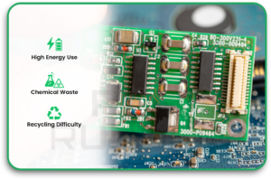
Today, most PCBs rely on copper as electrical conductors and silver-based metals for special conductive inks. Although they are reliable, these materials create significant environmental problems:
- The High Consumption of Energy Refining and mining metals requires a lot of energy.
- Chemical waste: Plating, etching and soldering generate hazardous waste that requires care in disposal.
- Recycling: The challenges: Metal and plastic layers are hard to separate, which makes recycling of boards difficult.
This growing concern has increased the demand for sustainable PCB materials that reduce chemical waste, energy use, and environmental damage during PCB manufacture.
What is Carbon Ink?
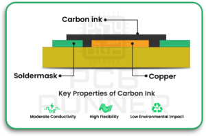
Carbon ink is a conductive compound made up of carbon nanoparticles or graphite. In contrast to metal-based inks, carbon ink avoids heavy metals and is generally considered more environmentally friendly than traditional metal-based conductive inks.
Key Properties of Carbon Ink
- Conductive suitable for low- to medium-current circuits
- Flexible, which makes it perfect for PCBs that are rigid and flexible.
- Recyclable and has a low environmental impact
Types of Carbon Ink
- Carbon inks with screen printing: Suitable for rigid and flexible boards
- Carbon inks that can be printed by an inkjet printer: Perfect to speed up the prototyping process of custom printed circuit board
- Carbon inks based on paste: Used in additive manufacturing as well as multilayer boards.
How Carbon Ink Supports Sustainable PCB Manufacturing
1. Lower Environmental Impact
- No heavy metals or toxic substances
- Reduces chemical usage in plating and etching
- Utilises less energy compared to traditional copper-based processes
2. Sustainability and Eco-Friendly Processes
- Work with additive manufacturing, such as the printing process of screen printing.
- Reduces the need for water and chemicals that are disposed of
- Allows eco-friendly PCB manufacturing processes while ensuring high-quality and reliability
3. Supports Circular Electronics
- It is easier to recycle than copper-based boards.
- Reduces the need for rare metals and supports environmentally sustainable electronic devices
Technical Advantages of Carbon Ink in PCBs
Electrical Performance
- Carbon ink is sufficiently conductive for applications that require low and moderate power, like sensors, IoT gadgets, and wearable electronic components.
- Although it isn’t as conductive as copper, it offers an unchanging and stable performance in the right application.
Flexibility and Mechanical Stability
- Carbon traces are less brittle than copper, which helps them tolerate bending and mechanical stress in flexible PCB applications.
- Their resistance to cracking under mechanical stress helps improve durability in flexible and wearable electronics.
Integration with PCB Manufacturing
- Compatibility with PCB manufacturing processes such as inkjet printing and screen printing.
- It is ideal for prototyping and small-batch manufacturing with minimal process adjustments required in standard PCB manufacture workflows, depending on the application and production method..
Carbon Ink vs Copper PCB
Understanding the difference between carbon ink and copper is critical for designers:
| Feature | Carbon Ink | Copper PCB |
| Conductivity | Moderate (suitable for low- to medium-current) | High (suitable for high-current) |
| Environmental Impact | Low | High |
| Flexibility | Excellent | Limited |
| Manufacturing | Additive printing, less chemical use | Etching, plating, higher chemical use |
For carbon-based conductive ink applications, this distinction helps designers decide when carbon ink is appropriate and when copper is necessary.
When to Use Carbon Ink in PCBs
Carbon ink is handy for:
- Wearable electronic circuits: Flexible, lightweight and low-power circuits
- Rapid prototyping Fast printing , custom circuit boards to be tested and re-tested
- Eco-friendly electronics: Devices where sustainability is the primary concern
- IoT and sensors: Low-power devices where the requirement for high conductivity is not necessary.
It is also helpful in hybrid or multilayer boards when it is used in conjunction with copper in order to lessen environmental impacts without compromising performance.
Best Practices for Using Carbon Ink
- Keep Patterns Minimal and even avoid continuous large areas. Small patterns that are evenly spaced ensure uniform conductivity.
- Combine with copper when it is required. Copper is a good choice for high-current lines, and carbon ink for circuits that require low power.
- Guard Traces: Use solder mask or protective coatings to avoid any damage from the assembly.
- Coordinate with Manufacturers: Check the specifications together with the PCB manufacturer partners to guarantee proper integration.
Limitations of Carbon Ink
- Conductivity is less than copper, making it not suitable for high-power or high-frequency circuits.
- Protection coatings are often required in extremely harsh environments.
- Scaling up for mass production is still in its development.
However, even with these limitations, carbon ink is an excellent choice for prototyping and flexible electronics as well as environmentally-friendly projects.
The Future of Sustainable PCB Manufacturing
The trend towards sustainability across Europe and around the world opens up potential for carbon-based conductive ink applications:
- Compliance: Regulations such as EU RoHS and REACH restrict hazardous substances, encouraging the use of alternatives to heavy metals in PCB manufacturing.
- Hybrid designs: Combining carbon ink and copper traces, it balances the environmental impact with electrical performance.
- New Carbon Inks Nanostructured carbon inks increase conductivity and expand their capabilities for use in custom printed circuit boards.
As regulations tighten across Europe, manufacturers are investing more in sustainable PCB materials like carbon ink to meet environmental and performance expectations.
FAQs About Carbon Ink in PCB Manufacturing
Q1. What is conductive carbon ink for PCBs, and why is it sustainable?
A: Conductive carbon ink for PCBs uses carbon instead of metals like copper or silver. It reduces energy consumption, chemical use, and waste, supporting sustainable PCB manufacture.
Q2. Can carbon ink replace copper in all PCB applications?
A: No. Carbon ink is best for low- to medium-current circuits. High-power or high-frequency circuits still require copper traces.
Q3. How does carbon ink affect custom printed circuit board manufacturing?
A: Carbon ink works with additive manufacturing like inkjet or screen printing, allowing prototyping and small-scale production with minimal environmental impact.
Q4. What are the main limitations of carbon ink in PCBs?
A: Lower conductivity than copper, potential durability concerns, and challenges in high-volume manufacturing.
Q5. What are some carbon-based conductive ink applications?
A: Flexible electronics, wearable sensors, IoT devices, eco-friendly consumer electronics, and prototyping for custom printed circuit boards.
Conclusion
Carbon ink is a sustainable option for PCB manufacturing in the modern age. It balances environmental responsibilities with high-quality performance for medium and low-power circuits. Although it isn’t able to replace copper in all aspects, it does provide an effective alternative to flexible electronic circuits, rapid prototyping and eco-friendly designs.
The use of carbon ink allows manufacturers and designers to develop eco-friendly PCB manufacturing processes and create robust, more eco-friendly custom printed circuit boards. The future of PCB fabrication is green, and carbon ink is leading the way.

