


Objective
Explain how Copper Coin PCB technology moves heat out of high-power boards, where it beats standard thermal management methods, and what to check before specifying it for a design.
Key Takeaways
- A Copper Coin PCB embeds a solid copper block inside the board layers to pull heat away from hot components fast
- It comes in two forms: buried, which sits under the component, and embedded, which links directly to inner copper layers
- Copper conducts heat far better than standard FR4, which is why coin integration outperforms thermal vias alone in high-power designs
- Common in 5G hardware, EV electronics, and any board where a small footprint has to handle a large thermal load
- PCB Runner fabricates Copper Coin PCBs up to 50 layers, built to IPC-A-600 standards
A board that runs hot in testing but passes on the bench rarely stays fine in the field. Push more current through a small footprint and the heat has to go somewhere. Thermal vias help, but past a certain power density they stop being enough.
That’s the point where most design teams start looking at copper coin integration instead of adding more vias or thickening the board. It’s not a new idea. It’s just one that gets reached for later than it should, usually after a thermal failure shows up in the field rather than during design review.
A Copper Coin PCB embeds solid copper directly inside the board layers to pull heat away from hot components faster than vias or thicker copper alone can manage. It comes in buried and embedded forms, each suited to different heat loads. Common in 5G, EV, and high-power battery applications where standard thermal management runs out of headroom.
What Is a Copper Coin PCB?
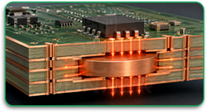
A Copper Coin PCB places a solid piece of copper inside the layers of a multilayer board, usually directly under or connected to a heat-generating component. Copper conducts heat far more efficiently than the FR4 or resin materials that make up the rest of the board, so the coin gives that heat a fast path out.
Standard heat dissipation methods, thermal vias, thicker copper layers, cooling fans, or specific soldering approaches, work up to a point. Once power density climbs past what those methods can handle, a solid copper coin gives the board a dedicated thermal channel instead of relying on distributed copper alone.
How Does a Copper Coin PCB Move Heat?
Heat moves from the component into the copper coin, then out through the board structure, either to the opposite side or between internal layers. The coin acts as a low-resistance path, similar to how a heat sink works, just built into the PCB stack instead of bolted on top of it.
This matters most in designs where the component itself sits close to its thermal limit. A few scenarios where this shows up:
- High-current power modules that heat up under sustained load
- RF amplifiers where thermal buildup affects signal stability
- LED drivers running at high brightness for extended periods
In each case, the coin doesn’t just move heat, it moves it consistently, which keeps the component’s temperature more stable under variable load than vias alone typically allow.
Buried vs Embedded: Which Copper Coin Type Do You Need?
The two types differ in where the coin sits and how directly it connects to the rest of the thermal path. Buried coins sit inside a pre-milled groove under the component. Embedded coins connect directly to the inner copper layers.
Buried Copper Coin PCB
- Lower processing complexity and lower manufacturing cost
- The coin sits inside the board but isn’t directly linked to inner copper, which limits how much heat it can move on its own
- Performance improves with high thermal conductivity fill materials, denser heat dissipation hole patterns, or thicker copper foil in the surrounding circuit
Embedded Copper Coin PCB
- Direct connection to inner copper layers activates faster, more consistent heat conduction
- Works well when the board needs to move heat away from a component the moment it’s under load, not after heat has already built up
- Typically the choice for higher power density designs where buried coins can’t keep pace
Neither type is universally better. The choice comes down to how much heat the design generates and how much that heat needs to move immediately versus gradually.
Where Does Copper Coin Technology Actually Get Used?
Copper Coin PCB technology shows up wherever a small board has to handle a disproportionately large thermal load. A few common applications:
- 5G network hardware: dense circuitry in compact enclosures generates heat that standard thermal management struggles to clear fast enough
- Electric vehicle electronics: power modules and battery management systems run hot under sustained load
- High-output, small-footprint batteries: where space constraints rule out bulkier cooling solutions
- Audio equipment: amplifier circuits that need stable thermal performance to maintain signal quality
The common thread across all four: limited board space combined with power levels that would overheat a standard FR4 layout without additional thermal support.
What Are the Real Benefits Over Standard Thermal Vias?
Thermal vias work by creating multiple small paths for heat to move through the board. They’re effective, but each via only moves a limited amount of heat, so high-power designs need a lot of them to keep up.
A Copper Coin PCB offers a few specific advantages instead:
- Faster heat conduction: a solid copper path moves heat quicker than an array of smaller vias
- Better process control: heat moves through a defined channel rather than distributed unevenly across many vias
- Support for high-speed communication: components run cooler and more consistently, which matters for signal integrity in fast-switching circuits
- More even thermal distribution: reduces hot spots that vias alone can leave behind in dense layouts
Copper conducts heat considerably better than the fiberglass-resin materials used in standard PCB substrates. That’s general electronics engineering knowledge, not a PCB Runner-specific figure, but it’s the underlying reason coin integration outperforms thermal vias once power density gets high enough.
What Should You Check Before Specifying a Copper Coin PCB?
Get these details confirmed with your fabricator before finalizing the design, since coin placement and PCB material selection both affect final performance.
- Layer count and coin placement: confirm how many layers the coin spans and where it sits relative to the heat source
- Base material: FR4 remains the standard base for most copper coin builds, though high-Tg variants matter for higher operating temperatures
- Metal thickness: inner and outer copper thickness affects how much additional heat capacity the surrounding circuit adds
- Registration accuracy: tight tolerances matter more with coin integration since misalignment affects thermal contact
- Compliance standard: confirm the fabricator builds to IPC-A-600 or an equivalent recognized standard
PCB Runner fabricates Copper Coin PCBs from 1 to 50 layers, with metal thickness ranging from half an ounce up to 6oz on both inner and outer layers, and registration accuracy held to 0.003 inches or tighter. Full specifications for this and other builds are covered on our PCB material page.
Copper Coin PCB vs Standard Thermal Via Design
| Factor | Copper Coin PCB | Standard Thermal Vias |
| Heat conduction speed | Fast, direct path | Moderate, depends on via density |
| Manufacturing complexity | Higher, especially embedded type | Lower |
| Cost | Higher for embedded, moderate for buried | Lower |
| Best suited for | High power density, compact boards | Moderate heat loads, standard layouts |
| Thermal consistency | High, even distribution | Can leave localized hot spots |
Conclusion
A Copper Coin PCB earns its place in high-power designs by solving a specific problem: getting heat out fast when standard vias and copper thickness can’t keep up. Buried and embedded coins each suit different thermal loads, so the right choice depends on how much heat your design generates and how quickly it needs to move.
If you’re working through a thermal design challenge on a current board, our team can review your layout against our Copper Coin PCB capabilities and confirm what fits. Submit your design files to sales@pcbrunner.com or engineering@pcbrunner.com, or call +44 203 2397011 to talk through your PCB fabrication requirements directly.
FAQs
Q. Does a Copper Coin PCB cost more to manufacture than a standard thermal via design?
Generally yes, particularly with the embedded type, since it requires more precise processing and layer alignment. Buried coins cost less but also move less heat, so the trade-off depends on your thermal requirements.
Q. Can Copper Coin PCB technology be combined with thermal vias?
Yes, and it often is. Many high-power designs use vias for general heat spreading and a copper coin for the specific hot spot under a power component.
Q. What base material works best with Copper Coin PCB construction?
FR4 is the standard base material for most copper coin builds. Higher Tg variants (like 170°C or 180°C rated FR4) matter when the board runs at sustained higher temperatures.
Q. How many layers can a Copper Coin PCB have?
PCB Runner builds Copper Coin PCBs from 1 up to 50 layers, depending on design complexity and thermal requirements.
Q. Is Copper Coin PCB technology only for high-volume production?
No. It fits both prototype and production runs, though tighter tolerances on registration accuracy matter more as layer count and coin size increase.



