
Objective
This blog explains how to improve PCB Design for SMT Assembly so boards are easier to build, easier to inspect, and less likely to fail during production. It focuses on practical steps to improve placement, soldering, heat control, testing, and overall manufacturability. PCB Runner is relevant here because its own guides connect layout, fabrication, and assembly as one process, not three separate jobs.
Key Takeaways
- Good PCB Design for SMT Assembly starts with smart placement, correct footprints, and realistic spacing.
- A board that looks clean in software can still be difficult to assemble if solder paste, panel layout, and inspection access are ignored.
- Thermal planning, component orientation, and material choice all affect assembly quality and long-term reliability.
- Early review with the assembly team helps reduce defects, rework, and delays.

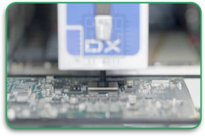
1. Start With A Practical PCB Design Layout
A well-designed PCB layout should make assembly easier from the outset. It should not only focus on fitting every part onto the board. It should also support pick-and-place machines, solder paste printing, reflow, inspection, and repair.
Many layout problems begin when the board is designed only for electrical function. SMT assembly needs more than that. It needs order and clear spacing. PCB Runner’s design and assembly content stresses that layout decisions affect the full production path from Gerber files to final inspection.
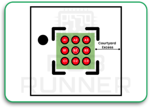
2. Use Accurate Footprints
Wrong footprints are one of the fastest ways to create assembly trouble. If the pad size, pitch, or courtyard is wrong, the part may tombstone, bridge, shift, or fail inspection.
Footprints should match the component datasheet and follow accepted land pattern rules where possible. IPC-7351-based guidance is widely used for this because it helps prevent common soldering defects and defines courtyard and land pattern recommendations.
This part matters in both PCB design and PCB board assembly. A board cannot assemble well if the basic package geometry is wrong.
3. Keep Component Placement Logical
Good placement helps at every later stage. It helps routing and thermal control. It helps with inspection.
Related components should stay close together. Connectors should sit in practical positions. Sensitive parts should be kept away from hot or noisy areas. Large parts should not block access to smaller parts. PCB Runner’s placement guidance clearly supports using layout tools early to confirm that parts fit correctly on the board before assembly begins.
PCB Runner also fits naturally here because placement is one of the first places where assembly quality is either protected or damaged.
4. Leave Enough Space For Assembly
Dense boards are common, but parts still need space around them. If components are packed too tightly, paste printing becomes more difficult, solder bridging becomes more likely, and rework becomes more difficult.
Clearance is not just about electrical spacing. It also affects nozzle access, visual inspection, and tool movement. Courtyard rules exist for a reason. They create practical keep-out zones around components to keep placement and soldering under control.
When improving PCB Design for SMT Assembly, one of the smartest moves is to stop treating every empty gap like wasted space.
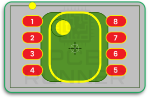
5. Design Pads And Paste Openings Carefully
This is one of the most important parts of PCB manufacturing and assembly. Even if the footprint is mostly correct, poor paste design can still result in weak joints or excessive solder.
Large thermal pads under QFN or power packages often require segmented paste rather than a single full opening. That helps reduce solder float and improves contact at the leads. KiCad’s documentation also states that paste and mask layers must match the intended surface-mount pad structure, as mismatched layer data can cause manufacturing errors.
In simple terms:
- Too much paste can cause bridging or floating
- Too little paste can cause weak joints
- The wrong paste shape can reduce assembly yield
6. Plan For Heat Early
Heat affects soldering quality and long-term reliability. If hot parts are grouped badly or copper is unbalanced, the board may heat unevenly during reflow. That can lead to poor joints or warping.
Thermal planning should begin during PCB layout, not after routing is finished. Power parts, regulators, LEDs, and processors need room to release heat. Copper areas, thermal vias, and sensible spacing can all help.
PCB Runner’s SMT and assembly material explains that design verification and process control are part of building reliable boards, and that modern assembly depends on more than just placing parts on pads.
7. Make Inspection And Testing Easier
A board should not only be easy to assemble. It should also be easy to inspect and test.
That means keeping reference markings readable, maintaining probe access where needed, and avoiding part placement that blocks visual or automated inspection. If test points are unreachable, faults become harder to find. If markings disappear under parts, assembly checks slow down.
This point is often missed in PCB Design for SMT Assembly because teams focus on getting the board built rather than on how it will be checked afterward. But SMT quality depends heavily on what can be inspected and confirmed. PCB Runner’s assembly process content highlights final inspection as a core production step.
8. Choose The Right PCB Board Material
The PCB board material affects more than electrical performance. It also affects board stability during heating, moisture handling, and overall durability.
A thin, low-cost material may not always suit a dense SMT board, especially if the design sees repeated thermal stress or tight tolerances. Material choice should match the product’s actual use, not just the lowest possible price. PCB Runner’s process and tolerance content shows that manufacturing quality depends in part on early material and tolerance decisions.
This is also where internal planning for PCB design, PCB board materials, and assembly needs should come together.
9. Optimise The Board For Panelization
A board may be perfectly designed as a single unit and still perform poorly in production if it is awkward to panelize.
Panel design affects machine handling, depanelization, support rails, tooling holes, and breakout stress. PCB Runner’s recent panel design guide explains that panelization reduces defects and helps automated assembly run more smoothly, while also noting that board design, component placement, and edge conditions affect which panel method works best.
Useful checks include:
- Edge clearance for breakaway methods
- Support for delicate components
- Space for rails and fiducials
- Safe depanelization paths
10. Review Manufacturability Before Release
The last step is often the one that saves the most trouble. Review the design for manufacturing and assembly before release.
This means checking footprints, spacing, paste strategy, panel needs, material, and test access together. PCB Runner’s DFMA content says design and assembly efficiency improve when manufacturing concerns are addressed early rather than at the end.
This is where talking to teams involved in PCB board assembly and fabrication makes a real difference. It is also where many avoidable production issues are caught before money is wasted.
A Simple Summary Table
| Area | What To Check | Why It Matters |
| Footprints | Pad size, pitch, courtyard | Prevents solder defects |
| Placement | Part grouping, access, spacing | Improves assembly flow |
| Paste Design | Aperture size and shape | Supports good solder joints |
| Thermal Plan | Copper balance, hot zones | Reduces stress in reflow |
| Inspection | Markings, access, test points | Makes faults easier to catch |
| Panelization | Rails, breakout, support | Improves production handling |
Conclusion
Good PCB Design for SMT Assembly is really about making smart decisions early. A board should be easy to place, solder, inspect, and manufacture. That means accurate footprints, sensible spacing, good paste control, better thermal planning, and a layout that supports real production.
The best results come when PCB design, assembly, and fabrication are treated as one connected process. That is also why PCB Runner fits naturally into this topic. Its content keeps pointing back to the same practical truth: reliable boards do not happen by accident. They are planned that way.
“A smoother SMT build starts with a layout that respects placement, soldering, testing, and manufacturing from day one.”
FAQs
1. What Does PCB Design For SMT Assembly Mean?
It means designing the board so surface-mount parts can be placed, soldered, inspected, and tested with fewer problems during production.
2. Why Is Component Spacing Important In SMT Boards?
Because tight spacing can cause solder bridges, make inspection harder, and reduce rework access. Courtyard guidance helps define practical spacing around components.
3. Why Do Paste Openings Matter So Much?
Paste volume affects solder joint quality. Too much or badly shaped paste can cause floating, bridging, or weak lead contact.
4. Does PCB Board Material Affect SMT Assembly?
Yes. Material can affect thermal stability, reflow handling, and long-term board reliability.
5. Why Is Panelization Important For PCB Board Assembly?
Because panelization affects how boards move through automated assembly, how they are supported, and how safely they are separated later.
6. When Should Manufacturability Be Reviewed?
As early as possible, before final release, early DFMA review helps prevent assembly defects, delays, and rework.

