Objective
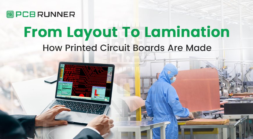
This blog explains how Printed Circuit Boards move from design files to finished assemblies. It breaks the process into simple steps so readers can understand what happens inside modern printed circuit board manufacturing, where quality risks appear, and why each stage matters before a board reaches final use.
Key Takeaways
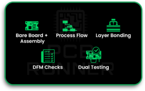
- Printed Circuit Boards are made in two main stages: bare board fabrication and PCB Assembly.
- A multilayer board starts with design data, material selection, inner layer imaging, etching, lamination, drilling, plating, solder mask, surface finish, and testing.
- Lamination is the step that bonds multiple layers into one solid board.
- Good manufacturing depends on strong design data and design-for-manufacturing checks before production starts.
- Testing matters at both the bare board stage and the final assembly stage.
What Printed Circuit Boards Really Do
Printed Circuit Boards hold and connect electronic parts. They create the electrical paths that let a product work. Without them, chips, connectors, and power parts would have no clean way to communicate. In simple terms, the board is the base, the road map, and the wiring system all at once.
There are two big stages in the journey. First, the bare board is fabricated. Then the board is populated with parts during PCB Assembly. That second stage is where the board becomes a working electronic product.
Did You Know? A multilayer PCB can go through dozens of production steps before it is ready for use. NCAB’s process overview describes more than 30 key steps in multilayer production.
Step 1: Starting With The Layout Data For Printed Circuit Boards
Every board starts as digital design data. This includes Gerber or image files, drill files, stackup details, copper weights, dimensions, and manufacturing notes. Before fabrication begins, the data is reviewed to make sure the board can actually be built. This is where design-for-manufacturing checks become important. Poor data at this stage can stop the job before it reaches the factory.
This is also where internal planning around printed circuit board (PCB) design matters. A strong layout makes later steps smoother, safer, and more predictable.
Step 2: Choosing Materials And Stackup
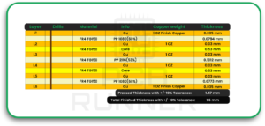
Next comes material selection. The manufacturer chooses the base laminate, prepreg, copper foil, thickness, and layer structure. In multilayer Printed Circuit Boards, this stackup controls board thickness, mechanical strength, and electrical behaviour. IPC guidance also treats material choice, copper foil choice, solder mask, and surface finish as key production decisions.
For some products, a standard rigid board is enough. Others may need a flexible printed circuit board for tight spaces or repeated bending. Flexible designs need different rules for bend areas and coating choices.
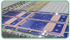
Step 3: Building The Inner Layers
For multilayer boards, inner copper layers are made first. A copper-clad core is prepared, imaged, and etched so the hidden circuit pattern appears on each inner layer. What remains is the copper that forms the real signal and power paths. This step must be accurate because these layers will later be sealed inside the finished board.
If an error slips in here, it can become costly because the defect may be buried after lamination.
Did You Know? Inner layers are made before the board becomes one solid panel. That means many critical circuits are created before the full board shape even exists.
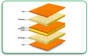
Step 4: Lamination Turns Layers Into One Board
Lamination is one of the most important steps in printed circuit board manufacturing. The prepared inner cores are stacked with prepreg and copper foil, then pressed together under heat and pressure. This bonds the layers into one solid panel. In simple words, lamination turns separate sheets into one multilayer board.
This step matters because it affects thickness control, layer alignment, and long-term reliability. A weak lamination process can create problems that are hard to fix later.
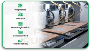
Step 5: Drilling The Holes
After lamination, holes are drilled where vias, mounting points, and component leads will go. NCAB explains that after drilling, the hole walls still have no metal deposit. At this stage, they are only mechanical holes. They do not yet carry electrical signals between layers.
Drilling accuracy matters for:
- Via position
- Hole size
- Layer registration
- Component fit
- Final reliability
This is one area where experienced pcb circuit board manufacturers can make a big difference.
Step 6: Copper Plating Creates Electrical Paths
Once the holes are drilled, they are metallised. A thin chemical copper layer is added first, followed by electroplating to build up copper where it is needed. This is what creates electrical continuity through the hollow walls and links one layer to another. NCAB notes that electroless copper creates the first thin deposit, and further plating builds on that base.
Without this stage, a multilayer board would have separate copper layers with no working path between them.
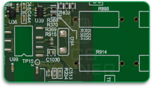
Step 7: Outer Layer Imaging And Etching
Now the outer layers are patterned. The manufacturer images the outer copper, develops the pattern, and etches away unwanted copper. This creates the final visible routing, pads, and copper features on the top and bottom surfaces. The process is similar in idea to inner layer imaging, but now it shapes the board’s outer circuit paths.
At this point, the board starts to look more familiar. You can now see where the components on a printed circuit board will sit later during assembly.
Step 8: Solder Mask, Legend, And Surface Finish
After the copper pattern is complete, the solder mask is applied. This protective layer covers areas that should not be soldered and helps protect copper from damage and contamination. NCAB describes common solder mask application methods such as screen printing or spray coating, followed by image transfer using UV exposure.
Next comes legend or silkscreen. This adds markings like reference labels, logos, and polarity signs.
Then the board receives a surface finish. IPC identifies surface finish as a core production choice because it affects solderability and storage behaviour.
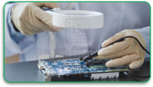
Step 9: Printed Circuit Board Testing
Before a bare board is approved, it is checked for faults. This stage may include electrical testing, visual inspection, dimensional checks, and process quality controls. Strong printed circuit board testing helps catch opens, shorts, registration errors, and surface defects before assembly starts. IPC’s training material for fabrication and assembly highlights quality control as a key part of reliable board production.
This is a very practical stage. It is far cheaper to catch a board defect before expensive parts are mounted.
Step 10: PCB Assembly Adds The Parts
After the bare board passes inspection, it moves to PCB assembly. Eurocircuits explains this as the second major stage after the bare board is made. Solder paste is applied, parts are placed, soldering is completed, and the finished board is inspected and tested.
This is where all the components on a printed circuit board are added, such as:
- Resistors
- Capacitors
- Connectors
- Chips
- Power parts
For buyers comparing printed circuit board manufacturers in the UK, it is useful to ask whether fabrication and assembly are planned together. That often reduces errors and saves time.
What Buyers Should Watch Closely
Not every problem starts in the factory. Many begin in the file package, stackup choice, or part plan. That is why the strongest printed circuit board manufacturing process usually includes early review of layout, materials, drill plan, finish, and assembly needs.
PCB Runner can support better results when design, fabrication, and assembly are treated as one connected process instead of separate jobs.
Conclusion
The journey of Printed Circuit Boards is more detailed than most people expect. A simple-looking board may pass through imaging, etching, lamination, drilling, plating, solder mask, finishing, inspection, and final PCB Assembly before it is ready to work. When each step is handled well, the board becomes easier to build, test, and trust in real products. That is why PCB Runner should look at the full path from layout to lamination, not just the final board in hand.
Looking at a new project? Start with a clear review of design files, materials, manufacturing details, and assembly needs before production begins.
FAQs
How Are Printed Circuit Boards Made In Simple Words?
They are made by creating copper circuit patterns on board materials, bonding layers together, drilling holes, plating copper through those holes, adding solder mask and finish, and then assembling components onto the finished board.
What Is Lamination In Printed Circuit Board Manufacturing?
Lamination is the step where multiple prepared layers are pressed together with heat and pressure to form one solid multilayer board.
What Happens Before PCB Assembly Starts?
Before PCB Assembly, the bare board is fabricated, finished, and tested. Only after that are electronic parts placed and soldered onto it.
Why Is Printed Circuit Board Testing Important?
It helps find faults like opens, shorts, alignment errors, and other defects before the board moves into assembly or final use.
Do Printed Circuit Board Manufacturers in the UK Also Handle Assembly?
Some do, and some focus only on fabrication. It is often helpful to choose a process where fabrication and assembly planning work together.
Can Flexible Printed Circuit Board Designs Be Made Differently?
Yes. Flexible boards use different materials and design rules, especially in bend areas, because they must handle movement and shape changes.

