Electronics in 2026 are moving fast. Devices are smaller, chips run hotter, and designs pack more connections into less space. That pressure lands on the factory floor. Your product quality often depends on the PCB Manufacturing Technologies your supplier uses.
If you are working with a PCB manufacturing team or comparing PCB circuit board manufacturers, you will notice one thing. The best results come from the right process choices, not just “good parts.”
This article is for you if you:
- design a pcb board and want it to be built cleanly
- manage pcb board assembly and want fewer defects
- source from PCB manufacture UK vendors, and want to understand what makes one shop stronger than another
- want clear, practical explanations with no fluff
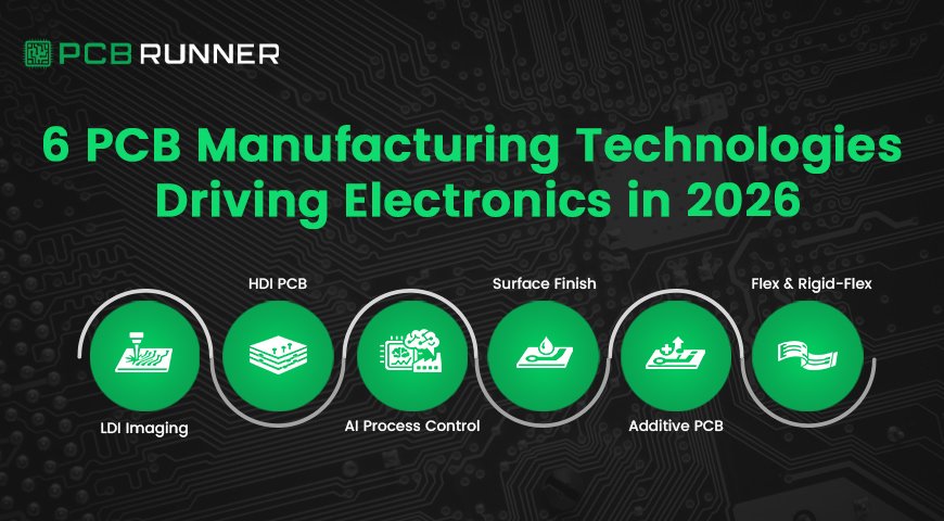
This blog will discuss six technologies that are shaping PCB Manufacturing Technologies in 2026, and what each one means for cost, lead time, and reliability.
Objective
To explain six manufacturing methods that are changing how a pcb board is built and assembled in 2026, using simple language and correct technical details.
Key Takeaways
You will learn:
- Why Laser Direct Imaging (LDI) helps fine features
- How HDI improves routing density using microvias
- How AI improves process stability in a PCB manufacturing line
- why surface finishes matter for fine-pitch pcb board assembly
- How additive and semi-additive methods help ultra-fine lines
- Why are flexible printed circuit boards and rigid-flex builds growing fast
Did You Know?
Many failures that occur during PCB board assembly actually begin earlier. A small misalignment, weak via plating, or the wrong PCB board material can lead to solder issues, intermittent faults, or early field failures. That is why PCB Manufacturing Technologies matter, even if you mostly think about assembly.
1) Laser Direct Imaging (LDI) for Ultra-Fine PCB Features
What Is Laser Direct Imaging
LDI images the copper pattern onto the photoresist using a laser. It replaces many of the film-based steps in traditional photolithography.
A simple way to think about it:
- Film imaging uses a physical film as a mask
- LDI writes the pattern directly with a laser
This improves repeatability, especially for dense boards.
Why LDI Is Critical in 2026
LDI is widely used because modern designs need:
- finer lines and tighter spacing
- better layer-to-layer alignment
- fewer imaging-related defects
If your printed circuit board (PCB) design includes small BGAs or dense routing, LDI can make the manufacturing result more predictable.
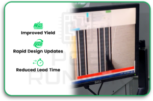
Key Benefits for Modern Electronics
LDI supports:
- higher yield and fewer defects
- quicker design changes (no film remake delay)
- shorter lead times for complex builds
These benefits show up later as fewer surprises in pcb board assembly.
2) Advanced HDI PCB Manufacturing Technologies
Evolution of HDI PCBs
HDI means High-Density Interconnect. The point is simple. You use smaller vias and tighter features so your pcb board can route more signals in less space.
In 2026, HDI has moved toward:
- more microvias
- more sequential lamination steps
- more complex via stacking in some designs
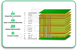
Key HDI Manufacturing Techniques
Sequential lamination
The board is built in stages. You laminate and drill, then laminate and drill again. This supports blind and buried vias, but increases process complexity.
Laser-drilled microvias and stacked vias
Microvias are usually laser-drilled. They often connect an outer layer to the next inner layer. Stacked microvias can reach deeper, but they need strong process control for reliability.
Applications Driving HDI Growth
Real products, not trends, push HDI:
- smartphones, wearables, and IoT
- automotive electronics with tight packaging
- AI hardware with dense routing needs
Many PCB circuit board manufacturers now treat HDI as normal work, not “special work.”
3) AI-Driven Process Control and Smart Factories
Role of Artificial Intelligence in PCB Manufacturing
AI in factories primarily focuses on monitoring and prediction. It monitors process data and flags drift before it becomes scrap.
Common areas include:
- etching stability (feature size control)
- drill accuracy trends
- plating thickness consistency
- assembly-line feedback, like solder paste printing drift
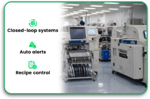
Smart Factory Implementation
Smart factories often use:
- closed-loop systems that adjust machines based on inspection feedback
- auto alerts when a process moves out of limits
- tighter control over recipes, so shifts produce consistent results
For a PCB manufacturing team, this reduces variation and improves repeat output.
Impact on Cost, Yield, and Reliability
When process control improves, you usually get:
- lower scrap
- fewer rework cycles
- more predictable lead times
- better reliability in the finished product
This matters whether you source locally or from PCB manufacturing options in the UK.
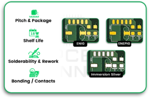
4) Advanced Surface Finish Technologies
Evolution Beyond Traditional Surface Finishes
Surface finish protects exposed copper pads and helps with soldering.
Traditional HASL can still work, but it has limits for fine-pitch parts. HASL can be less flat, and flatness matters for BGAs and small pitch components.
That is why modern PCB Manufacturing Technologies often use:
- ENIG
- ENEPIG
- immersion silver
Selecting the Right Finish in 2026
The finish choice depends on your design and assembly plan. Think about:
- component pitch and package type
- shelf life needs
- solderability and rework expectations
- any wire bonding or edge-contact requirements
A good finish choice reduces assembly defects and helps stabilise PCB board assembly yields.
Reliability Improvements for High-Performance PCBs
Better finishes help with:
- reduced oxidation
- stable contact performance
- improved solder joint consistency for fine-pitch parts
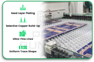
5) Additive and Semi-Additive PCB Manufacturing
What Is Additive PCB Manufacturing
Traditional fabrication is subtractive. You start with copper and etch away what you do not need.
Additive builds copper only where needed. That reduces waste and can support finer features.
Semi-Additive Process (SAP) for Fine Lines
SAP is common when you need very fine lines. A simplified view:
- Start with a thin copper seed layer
- Add copper where traces are needed
- remove leftover seed copper in open areas
SAP can support:
- very fine line width and spacing
- better line shape and uniformity
Use Cases in 2026 Electronics
You see SAP in:
- high-density builds
- high-frequency designs
- advanced packaging and substrate-like boards
Some PCB board materials work better with these fine-line processes than others, so material and process selection should be done together.
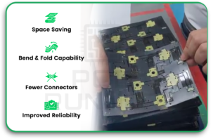
6) Flexible and Rigid-Flex PCB Manufacturing Advancements
Why Flex and Rigid-Flex Are Growing Fast
A flexible printed circuit board solves two common problems: space and movement. It can bend, fold, and reduce the need for connectors.
Rigid-flex combines rigid areas (for mounting parts) with flexible areas (for bending). It can improve reliability by removing connector points that can loosen over time.
Manufacturing Innovations in 2026
Factories have improved:
- lamination control between rigid and flex sections
- coverlay application quality
- bend area consistency and crack reduction
- dimensional control during processing
Industries Driving Adoption
Flex and rigid-flex are used more in:
- medical devices
- aerospace and defense
- automotive electronics
- wearables
They also change assembly planning, as fixturing and support during reflow must be properly designed.
How These Technologies Work Together
Most advanced boards use multiple methods.
A single printed circuit board (PCB) design might use:
- LDI for fine traces
- HDI microvias for dense routing
- a modern surface finish for tight pitch soldering
- AI-driven inspection to reduce scrap
- rigid-flex sections for packaging
Your real job is balancing:
- performance
- cost
- yield
- manufacturability
This is where early collaboration with PCB circuit board manufacturers helps.
Challenges in Adopting Advanced PCB Manufacturing Technologies
There are real hurdles:
- expensive equipment and setup
- process learning curves
- limited supplier capability for some technologies
- tighter design rules that require more planning
What PCB Designers and OEMs Should Prepare for
If you want fewer re-spins, do these early:
Choose your technology early
- Decide on HDI, surface finish, and flex needs before final routing.
Lock stackup and pcb board material early
- Material affects impedance, heat, drilling, plating, and reliability.
Update DFM and DFT
- Plan test points early.
- Confirm via structures and drill limits early.
- Keep assembly clearances realistic for machines.
Work closely with your manufacturer
- A short email at the end is not enough for advanced builds.
Future Outlook: PCB Manufacturing Beyond 2026
Expect:
- more automated inspection and handling
- stronger links between design tools and factory rule checks
- continued miniaturisation
- more focus on efficiency and sustainability
Conclusion: Technology as the Backbone of Electronics Innovation
In 2026, PCB Manufacturing Technologies decides what is possible in performance, size, and reliability. LDI, HDI, AI-driven control, advanced finishes, semi-additive methods, and flex/rigid-flex manufacturing are not “nice to have” anymore. They are often the reason a product works reliably.
If you are comparing suppliers, including PCB manufacturing options in the UK, focus on capability and process control, not just price. The right technology choices can protect your schedule and reduce defects in pcb board assembly.
FAQs
Which PCB technology is most important in 2026?
For many compact products, LDI and HDI are the biggest enablers because they support fine lines and dense routing.
Are advanced PCB technologies cost-effective?
They can be, especially when they reduce rework, scrap, and redesign cycles. Upfront costs may be higher, but the total project cost can drop as yield improves.
How do designers adapt to new manufacturing methods?
You adapt by selecting stackups and PCB board materials early, confirming via structures, using updated DFM rules, planning test access, and aligning with your manufacturer before final routing.
What industries benefit the most?
Wearables, smartphones, automotive electronics, medical devices, aerospace systems, and AI hardware benefit from compact, dense, and reliable PCB designs.

