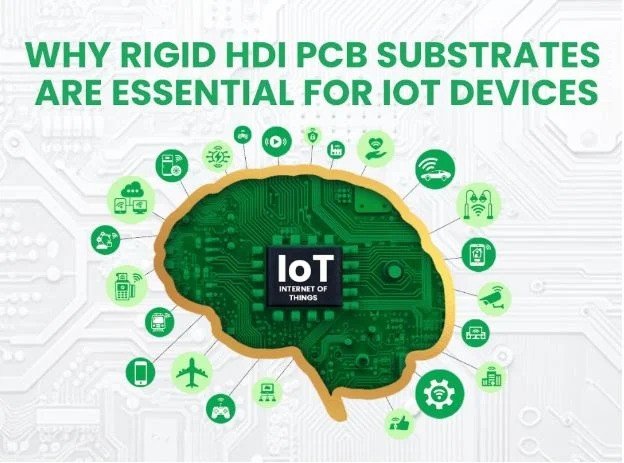
Why IoT Devices Rely on Rigid HDI PCB Substrates
The Internet of Things (IoT) is improving at a rapid pace, and there is a need for faster, more compact, and reliable products. The need for per unit surface area has risen drastically, which sets the goal for Rigid HDI (high-density interconnect) PCBs.
These new PCBs make it easier for designers to fit more functionality into a smaller space, which is more important than ever for constrained and cluttered IoT applications. With the increase of connected devices, it is important for all individuals targeted at IoT development to understand the relevance of Rigid HDI substrates.
In this blog, we will discuss HDI PCB fabrication, the performance and miniaturization of Rigid HDI PCBs enabling IoT devices, their advantages, and the reasons they are essential for modern electronics.
What Are Rigid HDI PCBs?
High Density Interconnect (HDI) PCBs offer greater circuit density in a smaller area due to the inclusion of thin traces, small pads, and miniaturized vias.
These kinds of PCBs are designed to transfer signals quickly. They feature advanced micro vias, buried vias, and blind vias to achieve compact and complex designs.
Rigid HDI PCBs are ideal for IoT devices as they provide advanced features. Their higher I/O counts, smaller size, and better performance make them suitable for multilayer boards.
In IoT, the Benefits of Rigid HDI PCBs are:
- Improved signal: Smaller vias greatly improved performance in high-speed IoT applications by reducing signal degradation.
- Miniaturization: HDI boards allow smaller electronic devices to be designed with a higher level of functionality. This is perfect for portable devices, wearable goggles, and many other devices where space is constrained.
- Cost Efficiency: The rigid HDI PCBs housing multiple components in a single unit allow for a drastic reduction in the number of components.
- Increased Reliability: Reducing the number of components and making the electrical connections stronger increases the performance and durability of IoT devices.
Application and benefits:
Including HDI PCB prototypes in your IoT designs helps achieve better signal integrity, compact form factors, and enhanced connectivity. Smart home systems, healthcare sensors, and wearable gadgets are all IoT devices that rely on increasing their overall performance while reducing their size.
Fitting several devices and their connections into one small board can greatly reduce costs and improve the time taken to manufacture new IoT products.
Expert Insights
Rigid HDI (High-Density Interconnect) PCBs are essential for IoT devices, offering superior performance in both compactness and functionality. As IoT technology demands smaller, more powerful, and cost-effective devices, rigid HDI PCBs provide the high-density interconnections needed to support advanced features in space-constrained applications.
These substrates are crucial for ensuring efficient signal integrity and thermal management, key aspects for IoT systems operating in diverse and often harsh environments. Additionally, the use of rigid HDI allows for the integration of fine-pitch components and complex routing, which are indispensable for modern, miniaturized IoT devices.
Moreover, rigid HDI PCBs enhance the durability and longevity of IoT devices by providing robust mechanical strength and moisture resistance. These boards excel in high-performance IoT applications, such as smart grids, autonomous vehicles, and medical devices, where reliability is non-negotiable. Their ability to withstand thermal cycling and environmental stress makes them ideal for IoT solutions that require long-term performance under varying conditions.
The combination of compact design, high thermal stability, and efficient manufacturing processes makes rigid HDI PCBs the go-to choice for cutting-edge IoT devices, enabling both functionality and sustainability in an increasingly connected world.
FAQs
Q1: What are the differences between HDI PCBs and other PCBs?
HDI PCBs have unique designs, offering greater electrical performance and higher-density interconnections compared to traditional PCBs, which have less efficient traces and vias.
Q2: Is it possible to use Rigid HDI PCBs for all IoT devices?
There is no question that Rigid HDI PCBs are flexible and can be fitted to various types of IoT applications, including wearable devices, smart home gadgets, and even industrial sensors.
Q3: How economical is rigid HDI PCB fabrication at mass scales?
Although HDI Rigid PCBs entail higher initial production costs than conventional methods, they become economical once multiple circuit boards are combined into one compact device, decreasing the number of additional parts needed.
Q4: How can Rigid HDI PCB enhance the efficiency of the signals?
Because of their distinct characteristics, advanced HDI PCB construction techniques such as microvias and blind vias can truly benefit signal integrity in high-frequency settings. Microvias mitigate signal loss, and blind vias significantly reduce interference and crosstalk.
Conclusion
The market is trending towards low-cost, highly functional, fully integrated IoT devices. To stay competitive, adopting Rigid HDI PCBs will help improve your IoT product design, increase reliability, and improve the time to market.

