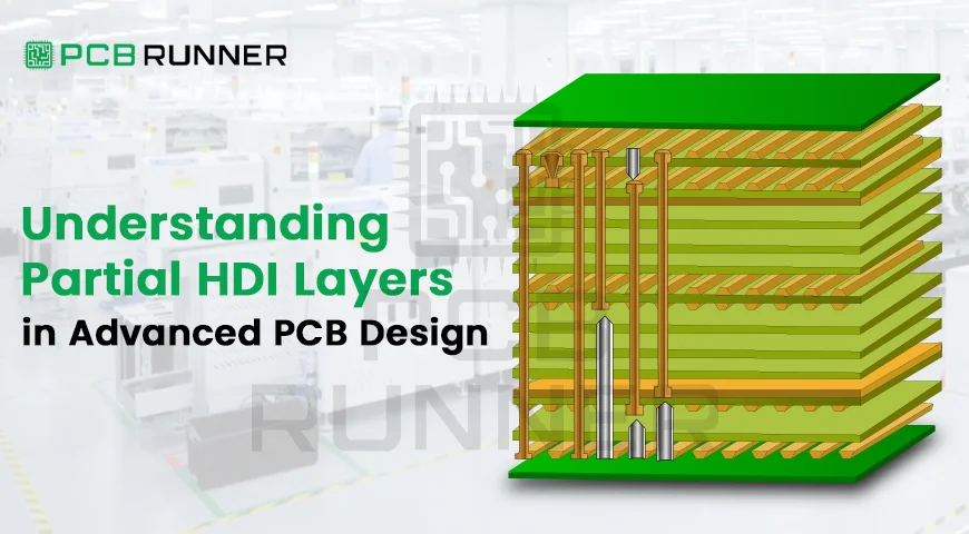
If you work with complex electronics, you already know how quickly things get tight on a circuit board. As parts shrink and features pack closer, you need layouts that move signals cleanly without extra noise or delay. That’s where partial HDI layers step in. They help you keep the board small, stable, and easier to build.
When designers talk with an hdi pcb manufacturer like PCB Runner, partial HDI often becomes the option that balances cost, space, and performance.
So let’s break it down in a simple and practical way.
What Partial HDI Layers Mean in High Density Interconnect PCB Work
Before HDI became common, boards had larger vias and wider traces. Things worked fine, but only when components were big. Modern parts don’t give you that space. A high density interconnect pcb relies on smaller features to open up routing paths without making the board thicker.
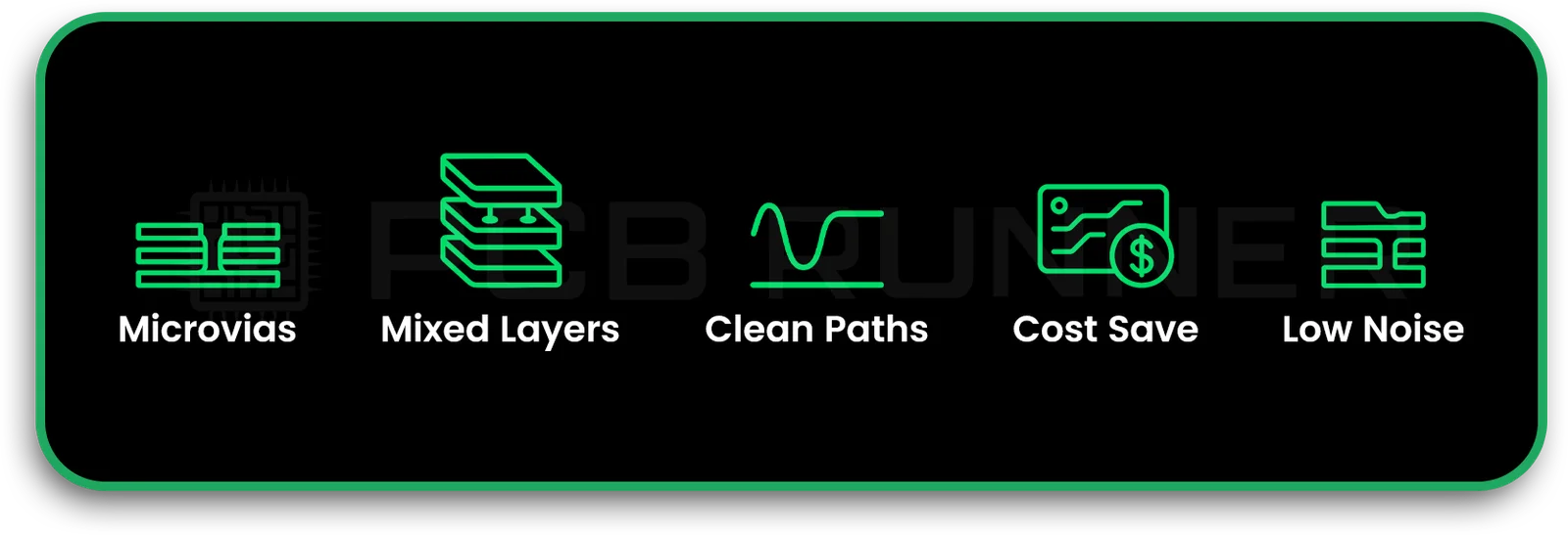
Here’s what partial HDI layers actually help you do:
- Add laser microvias only where you need them
- Keep the rest of the board on normal layers
- Control cost without losing performance
- Improve signal paths on crowded zones
- Reduce noise and keep signals clean
Think of it as building a road system. Not every street needs a highway. You only build the express lanes where traffic is tight.
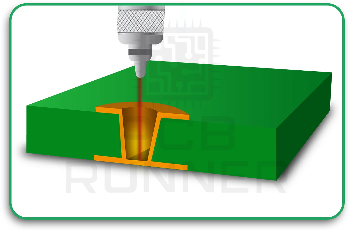
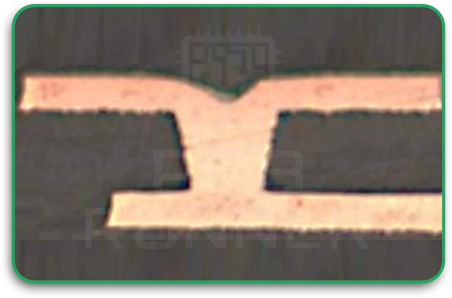
Why Laser Microvias Matter in HDI Printed Circuit Boards
Laser microvias are what make HDI layouts possible. They’re tiny drilled holes that connect one layer to the next. They are short, clean, and accurate.
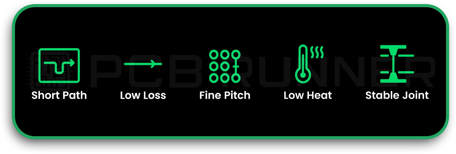
When laser microvias are part of the design, you get:
- Shorter electrical paths
- Less signal loss
- Better routing under fine-pitch parts
- Less heat build-up
- Small and stable joints
These benefits stack up fast in HDI printed circuit boards, especially when you’re working with tight packages like 0.5 mm BGAs.
HDI designers often rely on them because they keep the board layout under control, even when the component count is growing.
HDI Stackup Design and Why It Matters
Your HDI stackup design is the backbone of performance. Without the right stackup, even a strong layout can struggle.
What this really means is that every layer has a job. Some layers route fast signals. Others spread power. Others support microvias. When partial HDI is added, the challenge is to balance the HDI layers with the standard layers.
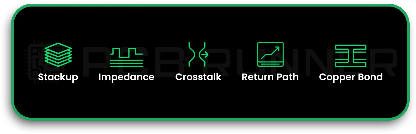
A smart HDI stackup design helps you:
- Keep impedance stable
- Shorten critical traces
- Reduce crosstalk
- Control return paths
- Maintain strong copper-to-dielectric bonds
Even one small mistake in layer planning can slow a signal or create noise. This is why manufacturers and designers usually plan the stackup first before placing any component.
When Partial HDI Layers Make Sense
Not every board needs full HDI. Many devices work perfectly with partial HDI because they only need microvias in limited zones.
You should consider partial HDI when:
- You’re routing under fine-pitch BGAs
- You want to shrink board size without raising cost too much
- Your design needs clean signal paths only on select layers
- You want faster routing around dense parts
- You want HDI speed without full HDI expense
Partial HDI layers help you fit everything neatly while keeping things reliable. For many teams, it ends up being the sweet spot between performance and budget.
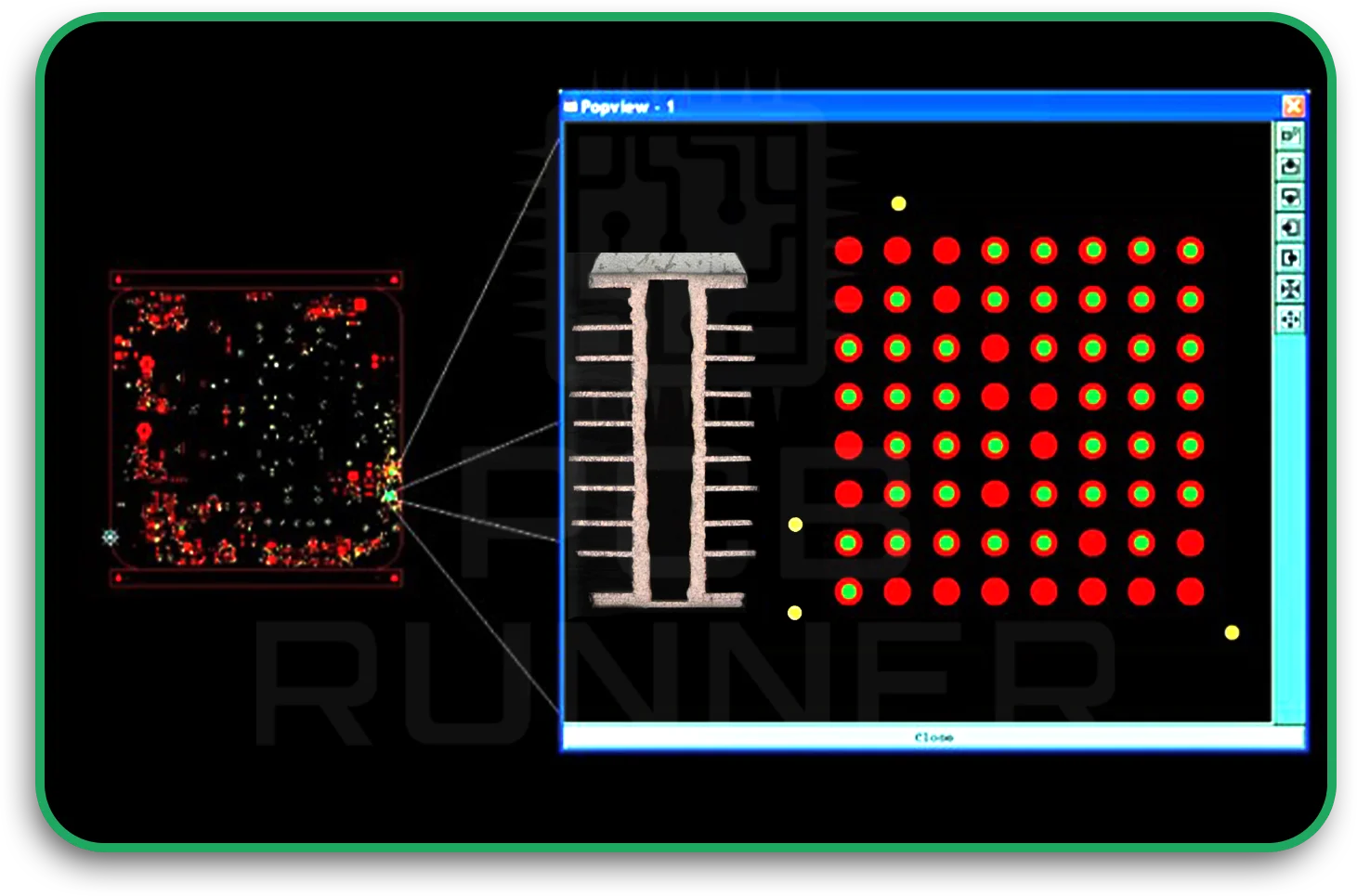
Common Types of HDI Vias You’ll See in HDI Printed Circuit Boards
Here’s a simple overview of vias in an HDI board:
1. Laser Microvias
These are the stars of high density interconnect pcb work. They connect thin layers with small, short paths.
2. Blind Vias
Blind vias link an outer layer to one or more inner layers without passing through the whole board. Think of them as shortcuts for signals. They help your signals travel a shorter distance, which lowers noise and keeps performance stable.
3. Buried Vias
Buried vias stay hidden inside the board. They connect only the inner layers and never reach the surface. These are useful when you need extra routing space inside the board but don’t want to disturb the outer layers.
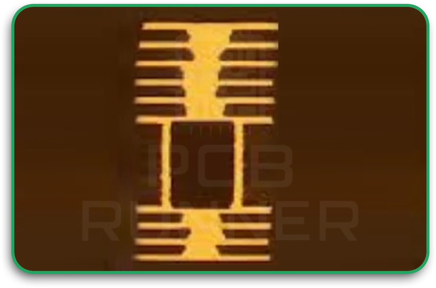
4. Via-in-Pad
Via-in-pad places the via right under a component pad. This method works well when you’re dealing with tight BGA layouts. It also helps move heat away from the component and makes routing much easier.
Each via type has a purpose. In partial HDI structures, designers often mix them to get the right balance.
Materials That Work Best With Partial HDI Layers
Material choice affects how microvias hold, how heat spreads, and how signals move.
Your hdi pcb manufacturer will usually suggest materials that match the size and density of your layout.
Good materials for partial HDI include:
- Low-loss laminates that support high-speed signals
- Thin dielectric layers for stable microvias
- Copper foils that bond well during lamination
- Resin-coated foils for strong microvia formation
Thin materials help keep laser microvias clean and short, which is key in advanced designs.
Tips to Improve Your HDI Stackup Design
If you want your HDI stackup design to work well without surprises, here are some simple habits you can follow. These are things you can apply right away, no matter how complex your layout looks.
Focus HDI Features on the Tightest Spots
Start by placing your HDI features only where you truly need them. The most common trouble spots are under BGAs or chips with a lot of pins. These areas demand tighter routing, so it makes sense to use partial HDI here instead of across the whole board.
Keep Microvias as Short as You Can
Short microvias usually give you cleaner and more reliable signals. The longer they get, the more room there is for loss. Keeping them short also helps with reliability during drilling and plating.
Aim for Symmetry in Your Layers
Try to keep your layer stack as balanced as possible. When the structure is even on both sides, the board is less likely to warp during lamination. A balanced build also helps maintain signal performance.
Plan Proper Return Paths
Every fast signal you route needs a clear and steady ground path. If the return path is broken or too far away, the signal gets noisy. Planning this early saves you a lot of headaches later.
Don’t Add Microvias Just Because You Can
Microvias are helpful, but too many of them weaken the copper around those areas. Use them only where they serve a purpose. A cleaner layout almost always performs better.
Use Matching Materials Across Layers
Try to keep your materials consistent. Different materials expand at different rates when heated, and that mismatch can cause cracks or stress inside the board. Matching materials keep the board stable from build to final use.
Following these simple steps helps you avoid common mistakes and builds a stronger, more reliable PCB from start to finish.
How PCB Runner Uses Partial HDI Layers
When teams work with an hdi pcb manufacturer, they want clean communication and predictable results. PCB Runner uses partial HDI by placing microvia layers only where they give real benefit. This helps keep costs lower while supporting complex routing around small chips.
The approach also supports stable HDI printed circuit boards without forcing a full HDI build when it isn’t needed.
FAQs
- How do laser microvias help an HDI PCB manufacturer build better HDI printed circuit boards?
Laser microvias let an HDI PCB manufacturer drill very small and accurate holes, which is key when you’re working with HDI printed circuit boards. These tiny holes keep signal paths short and clean. They also make routing under tight parts much easier, especially when you’re dealing with partial HDI layers.
- What does HDI stackup design mean for a high density interconnect PCB?
An HDI stackup design is basically the plan for how each layer, material, and via fits together inside a high density interconnect PCB. When this plan is done right, your signals move smoothly, noise stays low, and the board remains stable even when microvias are placed in partial HDI sections.
- When should you choose partial HDI for HDI printed circuit boards?
Partial HDI works best for HDI printed circuit boards that use fine-pitch parts like 0.5 mm BGAs. It gives you the routing support you need without making the board more expensive. An HDI PCB manufacturer often recommends partial HDI when you need high performance but also want to control cost.
- What are the perks of via-in-pad in HDI printed circuit boards?
Via-in-pad helps you route under tight parts in a high density interconnect pcb. It also improves heat control and helps an hdi pcb manufacturer create cleaner fanouts on partial HDI layers.
- How do blind vias and laser microvias work together in HDI stackup design?
Blind vias connect outer layers to inner layers, while laser microvias create short jumps between thin layers. Together they make an HDI stackup design cleaner and reduce noise in partial HDI structures.
- What materials work best for laser microvias in an HDI PCB manufacturer’s process?
Thin, low-loss materials support stable microvias in an hdi pcb manufacturer’s build. These materials help maintain strong bonds and smooth surfaces during the HDI stackup design process.
Conclusion
Partial HDI layers give you a simple and effective way to handle complex routing without raising costs more than you need to. By placing microvias only where they make a real difference, you keep your layout clean and your board stable. When you work with a team like PCB Runner, you can shape your high density interconnect pcb in a way that fits both your performance needs and your project budget.

