Over the past few years, printed circuit board technology has advanced dramatically. It demands goods that are both faster and more compact. HDI boards are considerably smaller now. They have tiny pads, copper traces, ultra-fine vias, and gaps.
HDI-printed circuit boards have significantly higher wiring density per unit than traditional printed circuit boards. HDI PCBs are typically defined as printed circuit boards with micro vias, blind vias, buried vias, high signal functionality, and built-up laminations.
Thus, high-density layouts have denser wiring, resulting in lighter weight, fewer layers, and more condensed PCBs. Instead of using multiple PCBs in a device, a single HDI board is adequate to house the functionality of the prior boards.
- Finer lines and spaces < 100 um / 0.01 mm
- Smaller vias<150 um and capture pads <400 um / 0.40mm
- Higher connection pad density > 20 pads/cm2
- 120-160 average pins per square inch

Benefits of Rigid HDI PCB Substrates:
- Better electrical performance and signal integrity
- Lower noise and crosstalk, and lower EMI/RFI
- Smaller size and weight
- Cost optimization
- Reduced design time
- More reliable designs
- Complex and dense devices
- Compact PCBs
When designing an HDI PCB board, it is critical to keep important manufacturing and design challenges in mind. There are a few of the most commonly reported difficulties:
- More connections are required to finish the board.
- You must design smaller parts in a much narrower space.
- There are relatively few workplace areas.
- There is a restricted board workstation area.
- There are more parts on each side of the PCB layer.
| Features | PCB Runner’s Specialty |
| Number of layers | 4–22 layers standard, 30 layers advanced |
| Technology highlights | Multilayer boards feature a higher connection pad density than normal boards, with thinner spaces, smaller via holes, and capture pads, allowing micro vias to only penetrate specific layers and even be inserted in surface pads. |
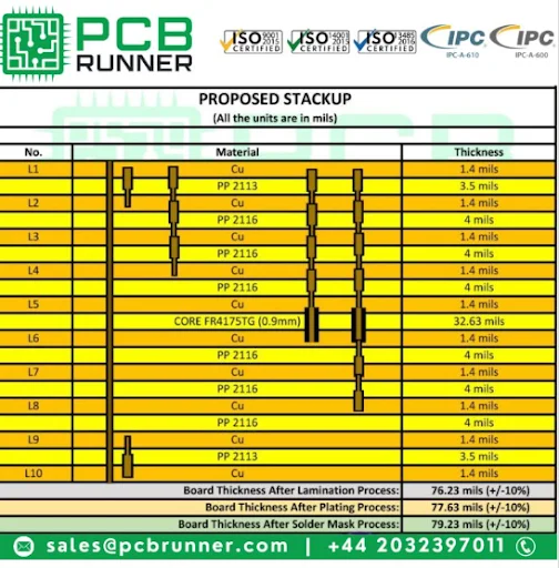
| HDI builds | 1+N+1, 2+N+2, 3+N+3,4+N+4, any layer or ELIC, Ultra HDI in R&D |
| Materials | FR4 standard, FR4 high performance, halogen-free FR4, Roger |
| Copper weights | 18μm – 70μm |
| Minimum track and gap | 0.075mm / 0.075mm |
| PCB thickness | 0.40mm–3.20mm |
| Maximum dimensions | 610mm x 450mm; dependent upon the laser drilling machine |
| Surface finishes | 0.10mm standard, 0.075mm advanced |
| Minimum mechanical drill | 0.15mm |
| Minimum laser drill | 0.10mm standard, 0.075mm advanced |
Types of Rigid HDI PCB Substrates:
A via is a tiny conductive hole that connects multiple layers of a PCB with a high density of interconnectivity. It provides signs so that one can pass across them with ease. Four different kinds of through holes penetrate into an HDI PCB, all of which are subject to PCB operations.
These are the following:
Blind Vias
To link the center layer of a multi-layered HDI PCB to the periphery, a drill or laser is used to punch the hole. The reason this hole is called the blind via is because it is only visible from one side of the PCB board. But keep in mind that this kind of hole is expensive and difficult.
Buried-vias
The multiplayer HDI PCB’s two inner layers are connected via the buried vias. It gets its name since it is always located on the internal surface of the printed electronics board and is invisible from the outside. A different drill file is needed for this via since it is also a plated hole. A buried passage has an even number of layers, such as 2, 4, 6, 8, and so forth.
Micro-vias
The micro vias, as their name suggests, are the smallest form, measuring less than 150 microns in diameter. A laser is also used to puncture it. These are among the most common kinds of vias used in HDI PCBs to connect one layer to the one next to it. In addition, its diameter is much smaller than that of mechanically bored vias, such as the through-hole. They are able to manufacture boards for electronics with more complex designs that are denser because of their size and ability to connect layers.
Via-holes
A drill or laser is used to drill this hole from top to bottom across the PCB. It facilitates the connection of the multi-layer PCB’s layers. Not only are they easy to build, but they are also among the most cost-effective options. To make them more inclusive, they have been separated into non-plated-through and plated-through holes.
Compared to microvias and through-hole vias, HDI technology offers a number of benefits, which include:
- Improved consistency: Compared to traditional PCBs, HDI PCBs are more trustworthy and less prone to damage since they contain fewer features and more densely packed interconnections.
- Improved performance: HDI PCBs are compatible for faster signal transfer, feature a greater number of connections, and provide improved performance for electrical devices.
- Higher densities of interconnections are supported by HDI technology, meaning that more superior connections can be constructed in a smaller space. It is essential for producing smaller and more complex PCBs.
HDI PCBs Structures:
HDI PCB (1+N+1): Simplest HDI
- One “build-up” of high-density connector layers makes up this HDI PCB structure, making it appropriate for BGAs with fewer I/O counts.
-
- It features great mounting stability and dependability, fine lines, registration technologies with a 0.4 mm ball pitch, microvia, and the potential for copper filled via.
- Applications: GPS, memory card, MP3 player, and cell phone.
HDI PCB (2+N+2): Moderate Complex HDI
- Two or more “build-up” of high-density connection layers make up the HDI PCB structure; microvias on various levels can be stacked or staggered; Copper-filled layered micro via structures are frequently found in difficult designs with demanding specifications for high-performance signal transmission.
- These can be utilized to boost routing density in a complex design while keeping a thin final board thickness; they are appropriate for the BGA with smaller ball pitch and greater I/O counts.
- Applications include game consoles, PDAs, cell phones, and portable video recorders.
ELIC (Every Layer Interconnection): Most Complex HDI
-
- All of the layers in this high-density interconnection (HDI) PCB topology enable free connectivity of conductors on any layer via copper-filled stacking microvia structures.
- This produces improved electrical characteristics and offers a dependable connectivity solution for extremely complicated big pin-count gadgets, such as CPU and GPU processors used in portable and mobile devices.
- Applications include memory cards, MP3, GPS, cell phones, ultra-mobile PCs, and compact computers.
Why choose our Turnkey Manufacturing?
PCB Runner offers turnkey solutions which include custom design layout, fabrication, components procurement & assembly labor, for all industries. Our expert design layout team efforts help the end R&D engineers/ Buyers/ Purchasers to reduce their time by going back & forth to design PCBs based on manufacturing capabilities & running DFM & DFA twice.
You are welcome to submit your design files to our email at sales@pcbrunner.com or engineering@pcbrunner.com


