Guide to Printed Circuit Board (PCB) Stencils
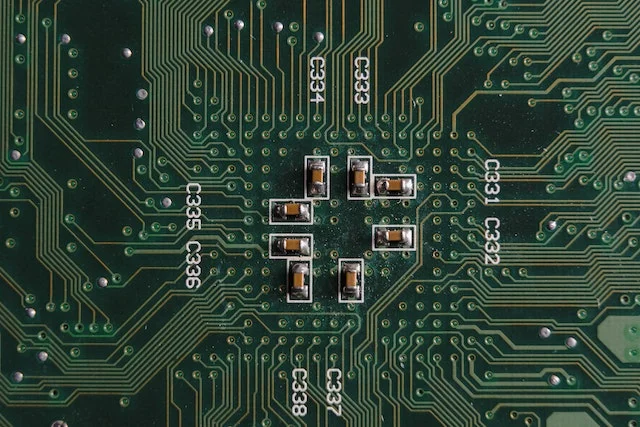
A printed circuit board (PCB) stencil is a thin metal sheet with laser cutouts used to apply solder paste to a PCB. The solder paste is a mixture of metal solder and flux that connect surface mount components to the PCB. The following is a guide to PCB stencils:
Stencil Thickness:
The size of the components used in the printed circuit board and the complexity of the design affect the stencil thickness. Thicker stencils are more robust and will last longer, but thinner stencils are more flexible and easier to use.
Stencil Design:
CAD software creates the stencil design, which generates a file in Gerber format. The Gerber file includes the paste layer needed to make stencil cutouts. Some stencil manufacturers like PCB Runner offer design services, so you can send them your PCB design files, and they will create a stencil design for you.
Stencil Production:
Stencils can be manufactured in many different ways. The most prevalent techniques are chemical and laser etching. Laser and chemical etching are the most common ways. Laser cutting is faster and more accurate but expensive. Whereas chemical etching is slower, it is more cost-effective for small production runs.
Stencil Inspection:
Stencils must get checked for any defects or damage that could affect the solder paste application.
Stencil Storage:
PCB stencils are stored in a dry, cool place to prevent corrosion. Handling the stencil is essential to avoid bending or scratching the surface.
Stencil Application:
- Place the stencil over the PCB and align the cutouts with the SMD pads.
- Use a squeegee to spread the solder paste over the stencil and through the cutouts.
- Remove the stencil carefully; the PCB is ready for component placement and soldering.
PCB stencils are essential tools for producing high-quality PCB assemblies. With the right design, production, and usage, stencils can help ensure that the PCBs are reliable and functional.

