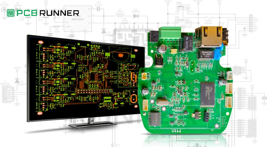
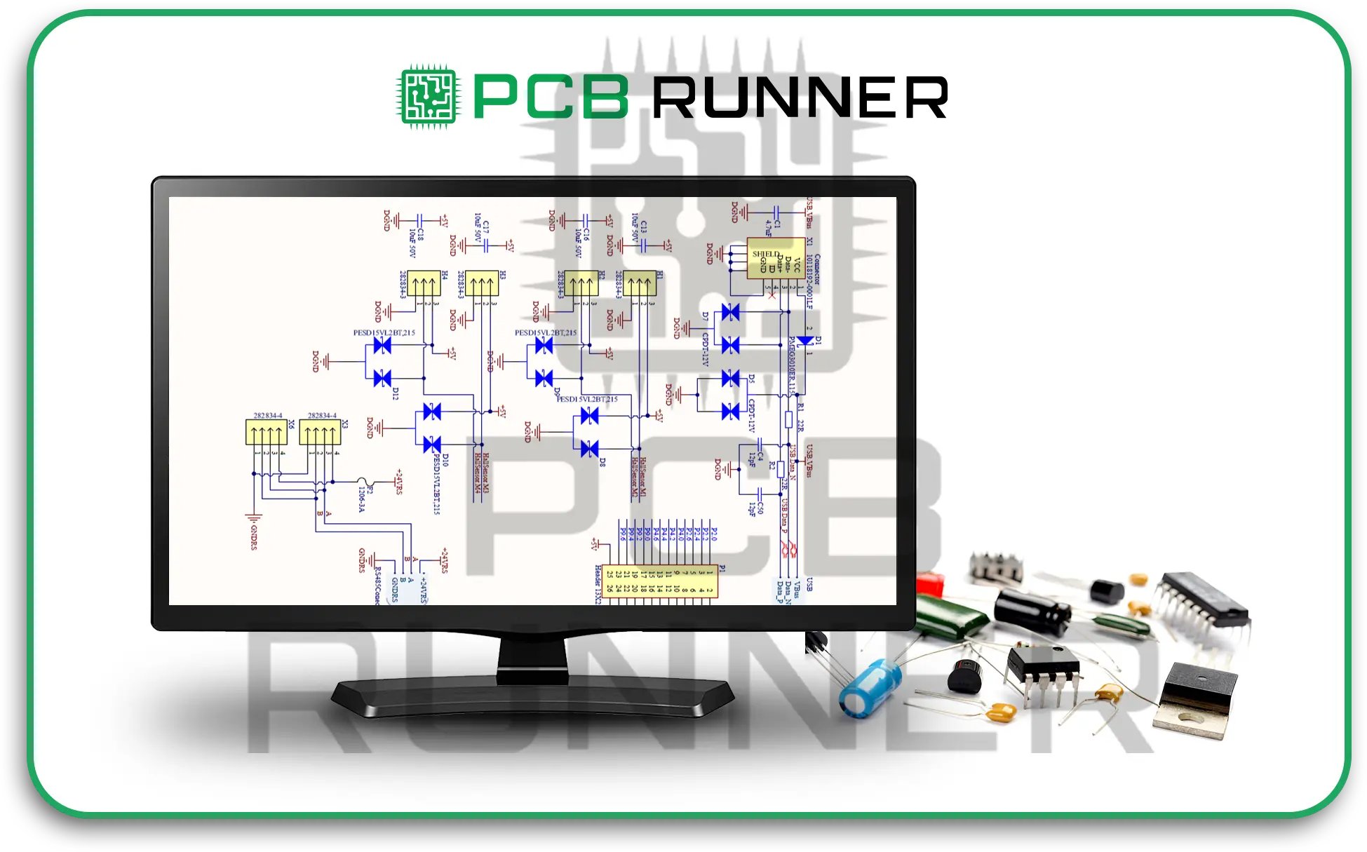
A printed circuit board (PCB) is an essential part of most electronic devices and systems today. A well-designed PCB enables seamless and dependable operation of the device, whether it is a simple gadget or a sophisticated aerospace gadget. Circuit engineers face the challenge of creating dependable circuits. The secret of a successful PCB is often found in the PCB layout design, which involves determining the placement of components and connections on the board. In this post, I will provide an in-depth PCB layout design guide to ensure efficiency and PCB reliability for devices and systems.
Components of PCB Layout Design System
Let us start with the fundamentals. A PCB consists of a flat, insulating board, with electronic components (like a capacitor, microchip and resistor) interconnected via a copper “trace” or “line.” The copper components share electrical pathways. The design layout shows the schematic diagram of the components and also provides an outline of the connections. A practical design layout will ensure the circuit operates as expected, can be produced through existing or novel manufacturing processes, and PCB reliability is guaranteed throughout the lifecycle.
What Is The Importance of PCB Layout?
Think about building a city; roads must be planned; otherwise, there will be traffic jams and accidents. The exact parallel applies to electronics, where there are traces that must be laid expertly so that signals do not weaken or interfere. These details and, more fundamentally, a good layout are a must to resolve underlying and potential issues.
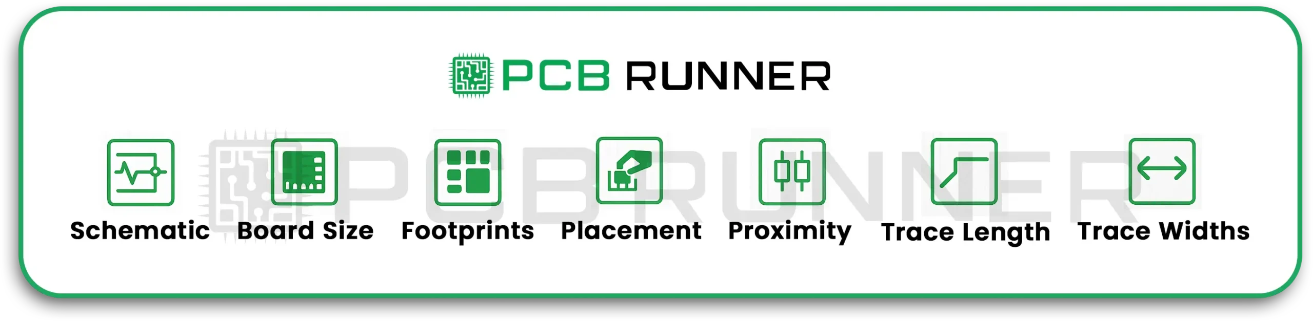
Best Practices for PCB Layout Design
1. Start with a Clear Schematic.
Before any parts are mounted on a board, you must first have a schematic diagram that shows every component and connection. The schematic portion is a guide for layout and helps you not miss any connections.
2. Define the PCB Size Early
Sketch and set the dimensions of the board and its shape first. Doing so allows you and the shape of the device or enclosure that you are working with.
3. Build or Use Standardised Component Footprints
Every component is represented on the PCB by a footprint that indicates the zone of the component to be soldered to the board. Use industry standards footprints to avoid any last-minute issues during assembly.
4. Thoughtful Placement of Components.
The component assignments are perhaps the most crucial portion of the circuit. Think of working on the layout as a puzzle; parts that help one another work must be grouped.
Keep Components Close to Minimise Voltage Drops
- Make sure to leave space in between components for heat to dissipate and for testing access.
- Avoid placing components in a way that makes assembling the circuit challenging.
Traces Should Be Short and Direct
- Short and straight traces are superior to long and winding traces as they minimise signal delay, noise, and loss. Long and winding traces are prone to interference and therefore affect the performance of the circuit.
Proper Trace Widths Should Be Used
Follow the manufacturer’s standard design rules on the width and spacing of copper traces to avoid overheating.
Work with your PCB Manufacturer to Determine Electric Needs
Signal integrity, impedance, and the resistance to signal flow are all affected by the arrangement of layers of copper and insulations. Work with your PCB manufacturer to get a stack-up that suits your circuit’s electrical needs.
1. Keep Analogue and Digital Sections Apart
Avoid mixing the noisy digital signals with sensitive analogue lines, as it will cause interference. In order to maintain signal clarity, set these sections apart in your layout.
2. Add Planes for Power and Ground
Solid copper planes are superior to traces when representing power and ground as they minimise electrical noise. The use of power and ground solid planes enhances stability.
3. Position Decoupling Capacitors Adjacent to ICs
Decoupling capacitors eliminate noise from power lines. For maximum effectiveness, ensure decoupling capacitors are placed as close as possible to the power pins of the chips.
Consider Manufacturing Constraints
The PCB has to be manufactured. These considerations regarding the design will help ease the fabrication of the board:
- Comply with the minimum spacing requirements.
- Do not place components where soldering is challenging.
- Select parts with industry-standard footprints to guarantee ease of procurement.
Your circuit board silkscreen should include designators, logos, and telltale markings like the reference designators, which tell the assembler where “pin one” is. These markings assist not only in assembly but troubleshooting as well which is invaluable in the repair process.
Adhering to Guidelines
Signal issues, overheating, and challenging manufacturability are common issues that arise when not following the provided guidelines. These are in place to ensure reliability. Your circuit will experience enhanced robustness and reliability to environmental factors, and ease of manufacturability for diverse production scales, most advantageous when a complete turnkey assembly is planned, where the board undergoes full build and thorough testing.
Considerations Based on Circuit Types
- High-Speed Digital Circuits: Maintain well-defined, controlled impedance paths.
- Analogue Circuits: Maintain a proper, digitally quiet zone with grounded physical distance to avoid interference.
- Power Circuits: Incorporate thermal reliefs on wide traces to mitigate the risk of overheating.
- Mixed Signal: Logically section the board and separate analogue and digital areas with controlled interconnections.
Your application’s requirements will profoundly influence the layout considerations.
Thoughts on Seeking Assistance.
The process of designing a custom printed circuit board (PCB) may become intricate. The careful review of your designs by experienced manufacturers and assemblers helps in correcting mistakes early on. They guarantee that your PCB fabrication assembly will adhere to your design intent and quality benchmarks.”
For instance, some firms will review your electronic board design files for free and provide prompt responses to queries around the clock. Working with a dependable PCB provider will assist in efficiently converting your circuit board layout into a tangible product.
Conclusion
Effective PCB layout design incorporates creativity and technical knowledge. It demands a systematic approach and a good grasp of the intricacies of electronic systems. Following these best practices, your custom printed circuit boards will be dependable for the entire life of your project: starting with unambiguous schematics, strategic component placement, meticulous routing, and trace routing alongside manufacturing considerations.
Those looking to deepen their understanding, resources like Cadence’s “PCB Design Layout Guidelines” explore achieving high-quality designs in significant detail.
As you approach the production and assembly phases, collaborate with seasoned manufacturers to guarantee that your PCB circuit layout will be transformed into hardware that operates as designed. For technical assistance and project support in professional-tier PCB manufacturing and assembly, specialised companies such as PCB Runner are a good fit.
For more in-depth PCB layout concepts, you may refer to Cadence’s blog on PCB design layout guidelines (Resource).

