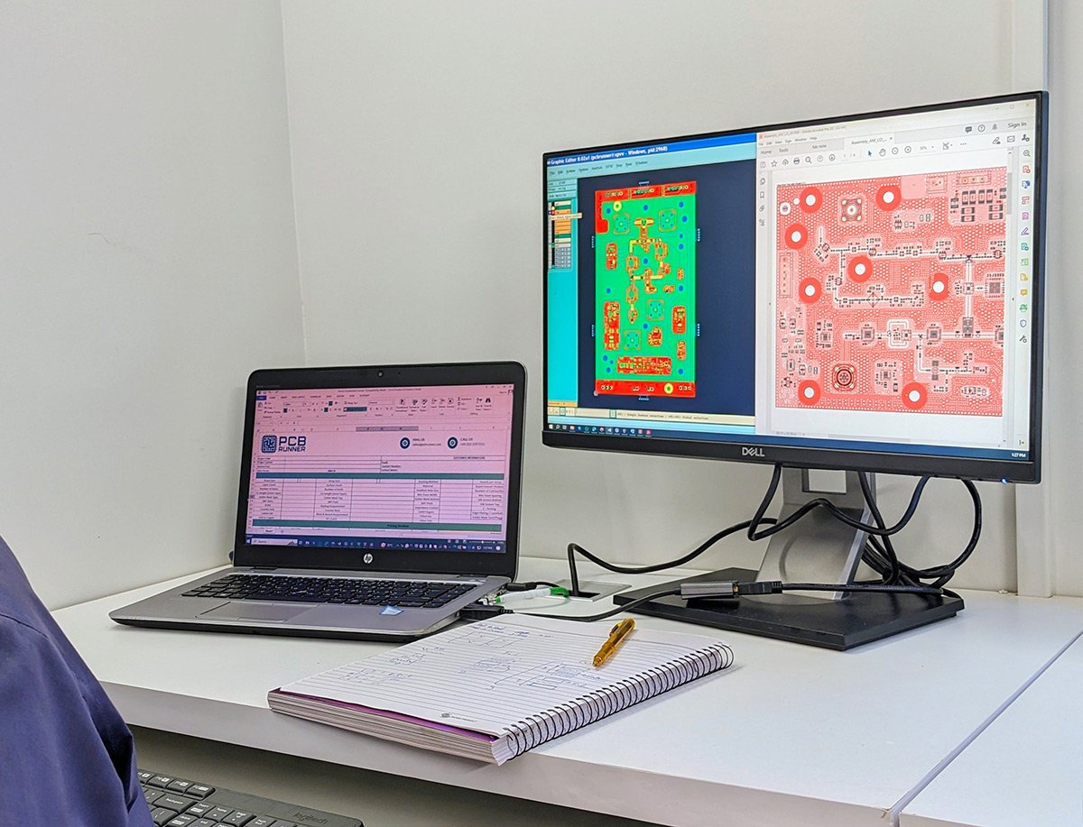
PCB Layout Design
PCB Layout Design Services UK and Europe
Our PCB Design Expertise In UK and Europe Includes:
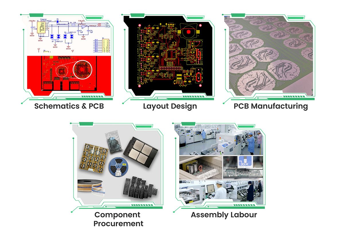
Schematic Capture and PCB Layout Designs for Highly Complex and Dense Boards
High-Speed PCB Design UK and Europe with Trace Length Optimization
We perform signal integrity services for high-speed circuit board designs. Moreover, we take care of cross-talk and controlled impedance requirements during PCB design and layout. Also we suggest use of PCB materials suitable for achieving a given set of signal integrity specifications.
Creation of all Types of Advanced Footprints and Libraries
Reverse and Re-Engineering Services
Checklist for PCB Designing
| 1 | SCHEMATIC DIAGRAM | |
| SOFT COPY (SOFTWARE NAME) | ||
| HAND DRAWN | ||
| 2 | BILL OF MATERIAL | |
| WITH MFG PART NUMBER | ||
| FOR FOOTPRINT PURPOSE | ||
| 3 | MECHNICAL DIMENSIONS OF PCB | |
| CRITICAL COMPONENT PLACEMENT, IF ANY | ||
| 4 | ENVIRONMENT OF PCB TO BE PLACED | |
| TO TAKE CARE ABOUT EMI/EMC/THERMAL | ||
| 5 | DESIGN CONSTRAINTS | |
| LIKE IMPEDANCE CONTROL, HIGH SPEED, | ||
| SPECIAL REQUIREMENT, IN ANY | ||
| 6 | IS THERE ANY KEEP OUT/NO GO AREA | |
| 7 | EXPECTED LAYER COUNT | |
| 8 | MAXIMUM VOLTAGE/CURRENT IN PCB | |
| FOR DETERMINING PCB PARAMETER | ||
| LIKE COPPER THICKNEES , CUTOUTS ETC. | ||
| 9 | SPECIAL INSTRUCTIONS, IF ANY | |
| 10 | LEAD TIME |
PCB Stack-Up Design
Factually, we always do an in-house stack-up design before starting on the layout design. It is just to make sure we have met all design objectives. Furthermore, we also recommend HDI technology to our customers if this is necessary, or could help in PCB optimization.
Cost Optimization
If you already have a PCB design and layout completed, we will gladly review it professionally for cost optimization. For instance, we try for layer reduction by using thinner traces closely spaced and smaller vias or by using laser-drilled micro-vias.
Please check out our PCB design review services.
Why Should You Get Your Circuit Board Design Done by PCB Runner?
PCB Runner believes in getting it right the first time. Therefore, we make sure there are no errors and omissions before we deliver your product. This saves our customers time, money, and the vicious cycle of changes and rectifications.
PCB Runner offers a completely customized PCB design and layout service. We also offer PCB prototyping and assembly services, which allows us to prove the design before taking up bulk manufacturing.
Reach Us Now
PCB Runner has over ten years of experience in PCB layout design, circuit board design, and PCB design and layout for a vast variety of cost-effective electronic products of high quality.
Success rates for our PCB design services in are high, as we follow good design practices. This allows quick turn-around times for our customers, and their time-to-market reduces substantially.
PCB Runner is a global supplier for quality PCB design services in UK and Europe.
You can request a free quotation at any time.
Our PCB Layout Design Capabilities
- Handling from 2 layers to 60+ layers and anything in between
- UL Certified laminates
- All types of through-hole and SMT design
- RF and Microwave circuits
- PCB design for commercial, medical, military, and aerospace
- Mixed Dielectrics
- High Density Interconnects
- Controlled Impedance
- Controlled depth back drilling
- Laser micro-vias
- Blind and buried vias
- Via in pads
- Bonded heat sinks
- Epoxy and Conductive via fill
- Plated edges and cavities
- Metal core PCBs
Our Major Expertise
We are experts at providing:
- High-density surface mount layout for µBGA, BGA, PCIE, PCI, CPCI, and more
- Rigid-flex circuit board designs
- Differential impedance control
- High-speed signal layout
- Ultra-low EMI/EMC design for MRI applications
- Sensitive analog circuit board design
- High-frequency PCB design and layout
- High current and high voltage design
- Design for Assembly
- Design for Manufacturability
- Professional documents for fabrication
- Design for Testability
- PCB assembly and prototyping
- PCB assembly and fabrication
- Testing PCBs
- Data generation for In-Circuit Testing
Our PCB design service is fully CAD based, and we use various PCB design software packages to meet the demands of our customers. We provide high level PCB design files conforming to the latest standards, and we our capabilities includes full 3-D design.
Standards we Follow
At PCB Runner, our PCB design and layout conform to the IPC 2200 Design Standard Series. We fabricate our completed designs according to IPC 6011 and IPC 6012. Also, we assemble our PCBs to meet the IPC-A-610 standards. Trust us; we perform all our activities in an accurate and timely manner and follow a schedule mutually agreed with our customers. Our focus for PCB layout design is to produce boards that offer our customers high yields, are easy to assembly and test.

