
Electronics get smaller every year. Your smartphone, fitness tracker, and car dashboard all pack more tech into less space. This miniaturisation happens because of microvias, tiny laser-drilled holes that connect different layers inside circuit boards.
If you design PCBs or work with an HDI PCB manufacturer, you know microvias can be tricky. One wrong move and your boards fail testing, cost more than planned, or break down in the field. At PCB Runner, we’ve seen these problems countless times.
This guide gives you seven practical tips for getting microvia designs right. You’ll learn how to avoid common mistakes and create boards that actually work. Let’s break it down.
What Are Microvias?
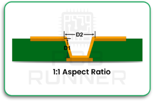
Microvias are small holes drilled with lasers, measuring 101.6 micrometres or (often ≤ 0.15mm diameter) used in HDI boards, with a 1:1 aspect ratio That’s thinner than two human hairs side by side. Microvias are mainly used in multilayer rigid, flex and semiflex PCBs.
Regular through hole vias drill across your entire board. Microvias only connect one or two neighbouring layers. This makes them perfect when you need tight routing in a high-density interconnect PCB.
Here are the main types of Micro Vias:
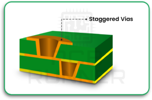
Staggered Vias: This is the most common and less costly method of implementing the Microvias to interconnect the multilayer high-speed or RF signals. By placing an offset on a slightly different axis, a zigzag path is created, as viewed through the cross-section of the stackup. And does allows multiple nets to be connected on a significant layer by ensuring length matching.
For full dimensional and design requirements, refer to the IPC-2226A HDI PCB design standard, defined under section 3.1.5
Stacked Vias: This is the costly method that involves placing microvias directly adjacent to one and another to form a stacked vertical interconnection with a critical tolerance. Stacked microvias are commonly used in designs where routing is not possible due to limited board area.
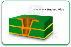
For full dimensional and design requirements, refer to the IPC-2226A HDI PCB design standard, defined under Section 3.1.4.
Microvias design best practices for HDI requirement:
There are several best practices which align with the guidelines and pros and cons for utilizing microvia structures in HDI stackups.
5 Essential Guidelines for Stacked vs. Staggered Vias
| Items | Stacked Microvias | Staggered Microvias |
| Space Efficiency | Beneficial to use in critical board dimensions or at high-density routing space. And save time for additional routing. | Takes significant time to decide placements and route to innerlayers. Requires more horizontal space for offset pads. |
| Reliability | High risk of failure under thermal stress if the dielectric and via locations aren’t chosen correctly. | Low risk of failures as offset design distributes stress evenly for thermal stress. |
| Cost | Expensive. | Less expensive but costly. |
| Signal Integrity | Excellent as it provides a direct vertical path and very ideal for high-speed or RF signals. | Excellent, however could need the extra work to length match and ensure impedance variations for longer paths across inner layers. |
| Manufacturing | Comes under ELIC Construction, requires strict tolerances and cross-sectional verification in every lamination step. | Easy to accommodate for the manufacturer, allows prepreg loss factor and requires cross-sectional verification in a specific lamination step. |
Wondering to know the tips from an HDI PCB manufacturer like PCB Runner for better microvia design best practices for your design requirements? Below we are covering the essential 7 tips which will help you out to make quick decisions.
| Tip | Best Practice | Why It Improves Microvia Design | Manufacturing Insights |
| 1. Microvia Structure: Optimize stacked vs staggered for reliability and high density | Use staggered where possible; limit stacking to ≤2 levels | Balances routing density with long-term reliability during thermal cycling | Stacked vias increase cost and stress; plating capabilities vary across fabs |
| 2. Aspect Ratios: Maintain proper aspect ratio and avoid plating failures | Target ≤1:1 aspect ratio (depth ≈ diameter) | Prevents voiding, thin plating, and electrical failures | Redesign stack or adjust thickness if aspect ratio cannot be met |
| 3. Landing Pads: Size land & capture pads correctly for drilling accuracy | Maintain proper land pad, capture pad, and annular ring geometry | Ensures drill hit integrity and protects yield in HDI layouts | Typical capture pad = 50–75 μm larger than via drill diameter |
| 4. Cost & Yield: Use microvias strategically to balance performance and costs | Apply microvias for BGA escape & dense routing; avoid overuse | Reduces defect opportunities and improves manufacturability economics | Combine standard vias + microvias for best cost-yield ratio |
| 5. Via Fill Method: Choose filling methods based on electrical, power & thermal needs | Copper-fill for power/thermal; resin-fill for signals; via-in-pad for density | Improves conductivity, thermal transfer & surface planarity | Not all fillers or via-in-pad methods are universally supported |
| 6. Stackup Approval: Co-design microvias and stack-up with PCB manufacturer early | Align drilling, material, and stack-up decisions before layout | Prevents redesigns & mitigates manufacturability limitations | Laser drilling accuracy differs by fabricator; documentation critical |
| 7. Signal Integrity: Consider SI, power delivery & thermal behavior | Use microvias to shorten stubs, reduce inductance & aid cooling | Improves high-speed performance & reliability | Essential for automotive, aerospace, telecom & HDI-dense applications |
Common Mistakes to Avoid
Even experienced designers mess up microvias sometimes. Watch for these:
Connecting too many layers with one microvia usually fails. Stick to one or two layers max.
Misaligned stacked microvias create stress and weak connections. Design landing pads with tolerance for some misalignment.
Wrong material combinations cause adhesion problems. Use materials your fabricator has tested together.
Wrapping Up
Getting microvia design best practices right takes attention to detail. These seven tips give you a solid foundation for creating reliable high-density interconnect PCB designs that manufacturers can actually build.
Pick structures that match your needs. Follow aspect ratio rules. Size pads for real-world tolerances. Use microvias strategically. Choose an appropriate filling. Collaborate early with your fabricator. Consider both electrical and thermal effects.
The PCB Runner engineering team helps customers navigate these choices every day. We’ll review your design during planning and catch problems before they become expensive.
Microvia technology keeps improving, too. Manufacturers develop better processes. Stay in touch with your fabrication partners to use the latest capabilities in high-density circuit routing.
With these essential tips, your microvia designs will work reliably and meet your performance goals.
FAQs
1. How many stacked microvias actually work in HDI PCB designs?
2+N+2 is getting common in 2026, however as per evolving manufacturing processes and designers needs. Pcbrunner capability allows to achieve up to 8+N+8.
2. Do microvias hold up in automotive HDI PCB applications?
Yes, if designed correctly. Keep a 1:1 aspect ratio, fill them appropriately, and validate with thermal cycling. Automotive designs demand tight process control.
3. Can microvias reduce EMI in HDI PCB layouts?
Yes. Their shorter length lowers inductance and improves return paths. Place them near signal transitions and ground connections for best results.
4. What’s the difference between copper-filled and resin-filled microvias?
Copper-filled microvias handle more current and heat. Resin-filled ones cost less and work well for signals. Both vias can typically be used in via-in-pad requirements..

