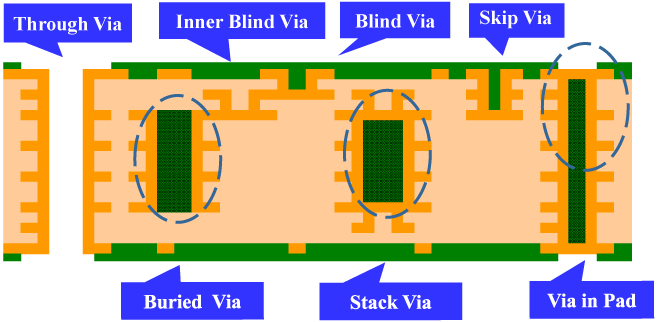
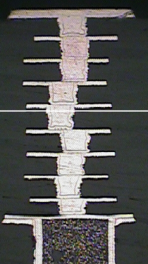
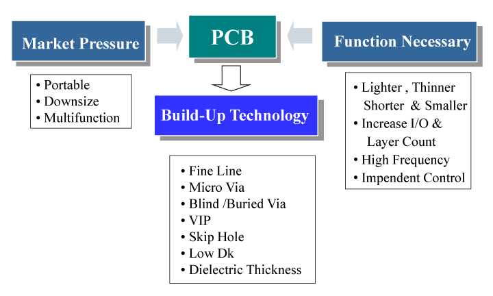
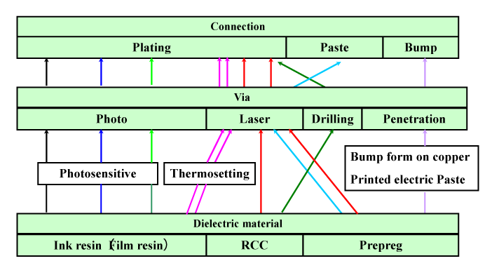
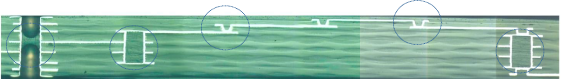
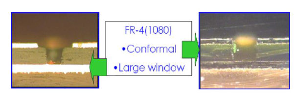
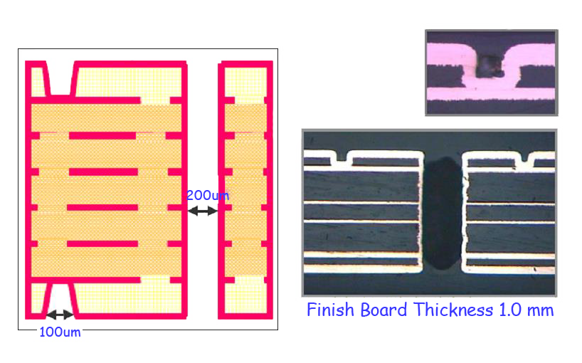
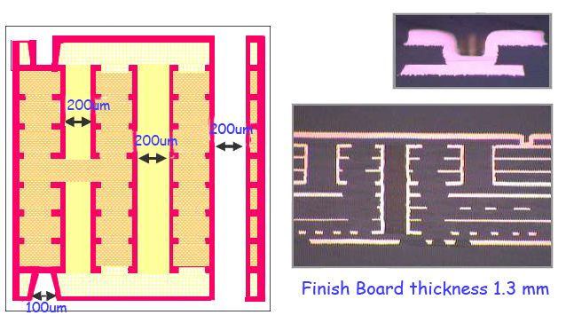
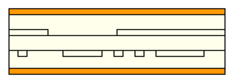
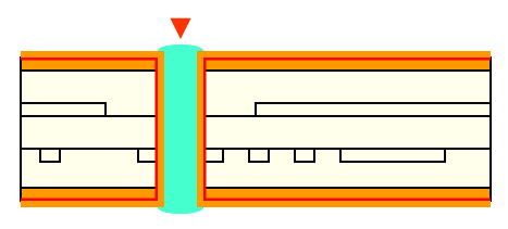
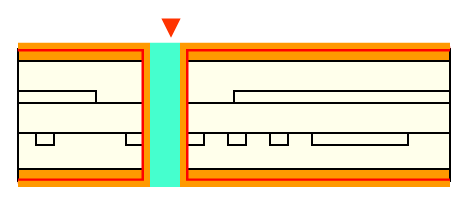
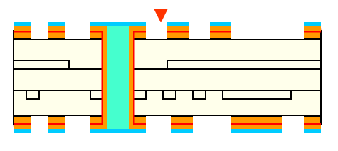
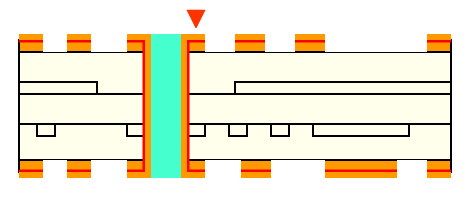
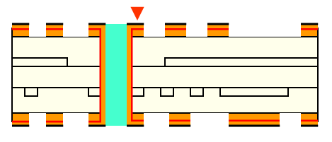
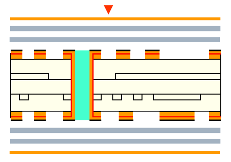
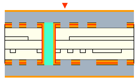
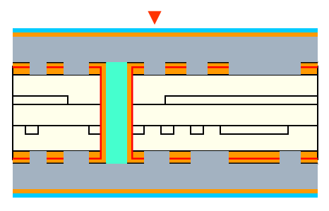
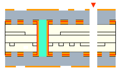
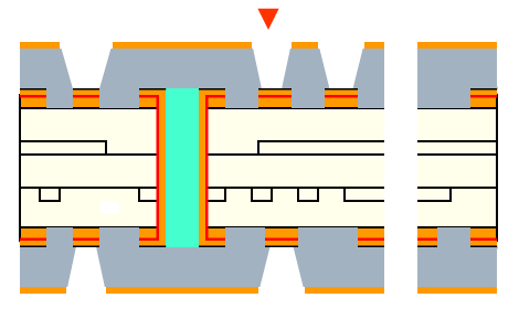
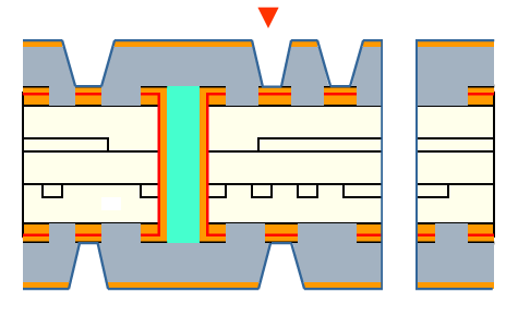
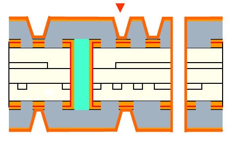
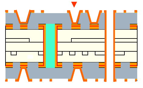
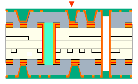
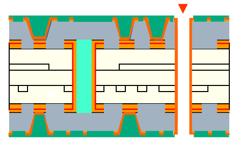
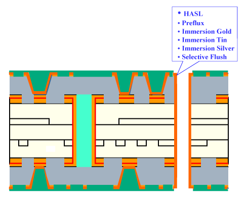
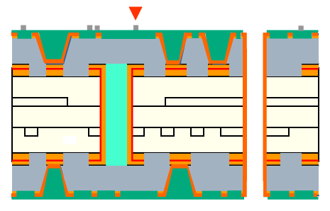
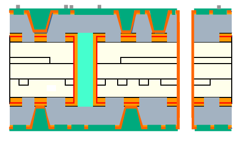
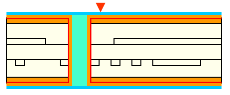
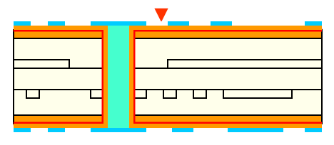
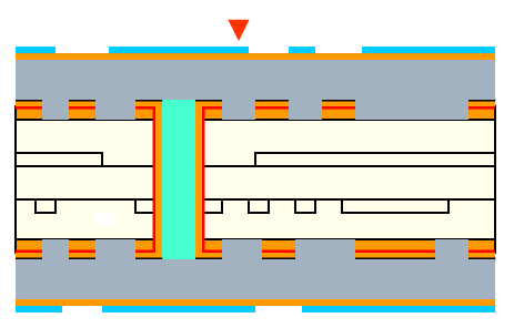
High Density Interconnection In Hole

Get a Free Quote Now


    HDI Technology in Hole

    High Density Interconnection

    Blind & Burried 9+2+9 Laser Drill

    Market Trend vs. Technology Solution

    HDI Process Flow

    Main Process of Build – up Layer

    Construction Materials

    Material Type

    • FR 4 Tetra Function ( Tg. 130 – 140 ℃ )
    • FR 4 High Tg ( Tg. 160 – 180 ℃ )
    • RCC ( Tg. 150 ℃ & Tg. 185 ℃ )
    • Ink ( VIL )

    Comparison of Material

    Prepreg RCC
    Low Cost ++
    Strength ++ +
    Hole wall roughness +
    Laminating control +
    Dielectric thickness 45um ~ 30um ~ 80um
    Smear residue on target pad ++
    Dielectric constant 3.9 ~ 4.7 3.2 ~ 3.8
    Shelf time ++ +
    Working PNL size ++ +

    Comparison of Via Technologies

    Mechanical Drilling Laser Drilling
    Low Cost in Equipment ++ +
    Low Cost in Production + ++
    Required Facilities Drilling Machine Laser Machine
    Consumable Drill Bits, Backup Board None
    Aspect Ratio 9 1
    Via Size Capacity 200 um~ 50~100um
    Speed 140 H/min 20,000 H/min
    Throughput +

    Comparison of Blind Via

    Prepreg

    RCC

    Build-up for 2 + N + 2

    Through Hole

    Inner Laser Via

    Stack Hole

    Inner Via Hole

    Surface Laser Via

    Laser Via Quality

    1+6+1 without buried, extend to 1+N+1

    1+4+4+1 with buried via, extend to 1+N+N+1

    2+4+2 laser via on laser via

    2+4+2 Staggered via, extend to 2+N+2

    Blind via Capability

    4- Layer Core Receiving

    I.V.H.(Inner Via Hole) Drilling

    Electroless Copper Plating

    Electro Plating

    Inner Via Hole Plugging
    ( for thickness >= 60 mil )

    I.V.H.Grinding
    ( for thickness >= 60 mil )

    Dry Film Lamination

    D.F. Exposure / Developing

    Etching

    D.F. Strip

    Black Oxide Treatment

    Prepreg Layup

    Lamination

    Dry Film Lamination

    D.F. Exposure / Developing

    Etching

    D.F. Strip

    Mechanical Drlling for TH

    Laser Drlling for Blind Via

    Desmear / Electroless Copper Plating

    Electro Plating

    Dry film, Exposure & DES

    Solder Mask Printing

    S/M Exposure / Developing

    Surface Finish

    Symbol Mask Printing

    Inspection

    laser-drilled micro-vias