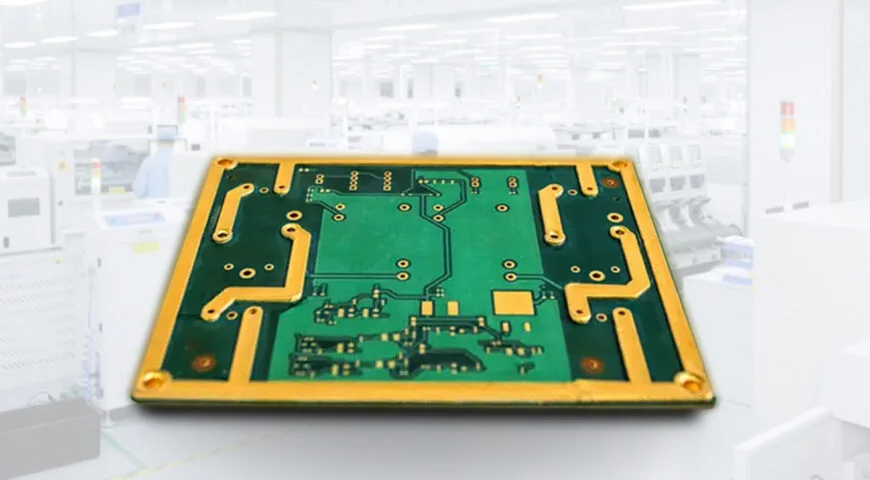
Heavy copper PCBs are crucial in industries that require durability, increased power, and enhanced heat dissipation. These specialized circuit boards are intended for power electronics, automotive systems, renewable energy, and industrial machinery and differ from standard PCBs by having thicker copper layers.
Top-tier PCB circuit board manufacturers have developed sophisticated fabrication methods for these boards across the industry, so they perform exceedingly well under challenging conditions. As an engineer or designer specializing in high-power applications, knowing the advantages of heavy copper PCBs and their manufacturing processes will allow you to optimize your design choices.
In this blog, we will discuss the fabrication techniques for heavy copper PCBs, their significance, and the most important aspects to look for in pc board manufacturers for your specific project.
What Is A Heavy Copper PCB?
Heavy copper PCBs have an enhanced copper layer thickness when compared to standard PCBs, leading to more functionality. While PCBs usually feature copper thicknesses around 1 oz/ft² (35 µm), heavy copper PCBs boast copper layers from 3 oz/ft² (105 µm) to beyond 20 oz/ft² (700 µm).
These boards are widely used in high-power and rugged operations such as power distribution systems, high-current circuits, and thermal management due to their durability and strength.
Highlights Of Heavy Copper PCBs
- Wielding Capacity for High Current
- Superb management of heat
- Better sturdiness
- Enhanced protection in harsh conditions
- Greater resistance to failure mechanisms due to thermal cycling
Heavy Copper PCB Manufacturing Process
The manufacturing process of heavy copper PCBs is more involved than that of standard ones. Because of the thicker copper layers, adhesion, etching, and plating techniques have to be specialized in order to achieve qualitative results.
1. Designing the PCB Layout
Engineers utilize sophisticated software for PCB design to outline the details of how they want the layout for copper thickness, trace width, and thermal functionalities, along with the degree of copper interconnects to be on the PCB. For intricate circuits, HDI or high-density interconnect technology is frequently used as well.
2. Selecting the Right Materials
Heavy copper PCBs are particularly made using base materials that can endure extreme temperatures and high mechanical stress. Thick copper supporting substrates, usually FR4 polyimide or even metalcore, are of high grade, enhanced middle grade offered in the market.
3. Copper Cladding and Etching
Heavy copper PCBs are different from their standard PCBs in that the copper layer is thick and requires a more complex approach to etching. The manufacturer has stepwise etching approaches to guarantee the etching is less than the required amount, and so the trace forms are workable.
4. Electroplating (Plated Through-Hole Technology)
This step helps build the electrical interconnections between heavy copper pads or traces and the plated through holes. For attaining reliable electrical connections for high-current applications, this step is important.
5. Lamination and Drilling Procedure
The first step in the Drilling and Lamination phase is the splicing operation. The copper layers that became previously etched must also be formed prior to mounting so that they add up together. After that, the layers are laminated under high temperature and pressure, and the CNC drilling machines then mount the holes for the components to sit.
6. Surface Finishing
Enhancements of the PCB’s durability and its ability to have components soldered onto it are done by applying HASL (Hot Air Solder Leveling), which is relatively cheap and commonly used, ENIG (Electroless Nickel Immersion Gold), which has excellent resistance to oxidation, and finally OSP (Organic Solderability Preservatives) which are cheap and eco-friendly.
7. Quality Control and Testing
Before removing the product from the soldering jigs, the manufacturers of heavy copper PCB perform systematic inspections of the workflow to ensure that it complies with the regulations of the industry. These checks normally consist of Automated Optical Inspection (AOI), tests to check whether the board is electrically conductive or contains short circuits, and thermally cyclic tests to check durability by varying temperatures.
Advantages of Heavy Copper PCBs
1. High Current Carrying Capacity
Heavy copper PCBs are specifically designed to accept greater magnitudes of electricity without suffering from excessive heating. They have thick traces of copper around the board that decrease the resistance, making the transfer of power very effective.
2. Excellent Thermal Management Heavy
Copper PCBs enable efficient heat spread and dissipation that prevents overheating and component failure. For this reason, industries with high-powered components are able to use these PCBs without worrying about the excessive heat being constantly generated from powering up the components.
3. Mechanical Strength Improved
Greater copper thickness improves the mechanical strength and durability of the PCB, which is now able to withstand thermal stress, vibration, and physical damage. This is crucial for automotive, aerospace, and industrial use.
4. Complex Designs Achievable With Fewer Layers
In conventional multilayer PCBs, extra layers are added to accommodate high power levels. When utilizing heavy copper PCBs, designers can meet current and thermal management constraints while also reducing layer count, thereby achieving cost efficiency.
5. Lifespan of the Product Increased
The durable structure of heavy copper PCBs facilitates their use over more extended periods, decreasing the need for replacements in mission-critical applications.
Industries that Heavy-Copper PCBs are used in
Heavy copper PCBs are integrated into those industries where high power, reliability, and durability are factors of a critical nature.
1. Power Electronics
- Power Converters
- Inverters
- Electric Power Distribution Boards
2. Electric Systems for Vehicles
- Electric Vehicle (EV) Power Systems
- Battery Management Systems (BMS)
- Charging Stations
3. Defense Electronics
- Radar Systems
- Satellite Electronics
- Military Grade Power Supplies
4. Electronics Energy Processing
- Solar Power Inverters
- Wind Energy Control Circuits
- Smart Grid Electronics
5. Automation Electronics
- Motor Control Units
- Automation and Robotics Systems
- High Power LED Lighting Systems
How to Choose the Right Shielding for Your PCB
Selecting the right PCB circuit board manufacturer for heavy copper PCB fabrication is essential to ensure high-quality performance.
1. Knowledge in Heavy Copper PCB Fabrication
Not all pc board manufacturers will work with heavy copper technology. Look for manufacturers who have thick copper layer handling experience.
2. Modern Fabrication Technology
Your PCB manufacturer should offer the following:
- High-Density Interconnect (HDI) technology
- CNC precision drilling and routing
- Complex custom pc board fabrication
3. Compliance with Procedures and Standards of Quality
Be sure that the manufacturer conforms to ISO, IPC, and UL standards for high-quality heavy copper PCBs.
4. Modification and Design Aid
An appropriate PCB supplier should be able to offer the following:
- Support with custom PCB layout design
- Advice on appropriate choice of materials
- Prototype testing prior to production in bulk
5. Quick Delivery and Efficient Supply Chain
For industrial or automotive use, as in other fields, prompt production and delivery is critical. Look for a supplier that has good logistical capabilities and can ship worldwide.
Final Thoughts
Heavy copper PCBs transform the capabilities of high-power and high-reliability products. Their capacity to carry large currents, shed heat, and be put under harsh conditions makes them vital in power electronics, automotive, aerospace, and renewable energy industries. With the knowledge of the heavy copper PCB fabrication process, you can decide more wisely which PCB circuit board manufacturers suit your project. Regardless of whether you need custom PCB fabrication or require mass production, an experienced pc board manufacturer will guarantee the desired quality.
Searching for Superior Heavy Copper PCBs?
At PCB Runners, we are experts in the fabrication of heavy copper PCBs utilizing state-of-the-art high-density interconnect (HDI) technology. Reach out today for a free quote on your project!
FAQs
1. What is a heavy copper PCB?
Unlike standard PCBs, a heavy copper PCB features thicker copper layers, usually between 3 oz/ft² and 20 oz/ft².
2. What are the benefits of using heavy copper PCBs?
They have remarkable current carrying capacity, exceptional thermal conductivity, heightened physical strength, and an extended operational life.
3. Which industries employ heavy copper PCBs?
They are extensively employed in power electronics, automotive, aerospace, industrial automation, and renewable energy sectors.
4. How do you select the appropriate manufacturer for PCBs?
Seek out companies that specialize in the production of heavy copper PCBs, high-density interconnect (HDI) technology, and have ISO/IPC credentials.
5. Where can someone obtain superior-quality heavy copper PCBs?
PCB Runners procures specialized heavy copper PCBs with sophisticated technological processes and rapid order fulfillment.

