Have you ever wished you could bring your electronic concept to life? The first step of that journey is usually a board, a PCB. But what if your concept requires a mix of portability, energy efficiency, and flexibility? In that case, double-sided prototype PCBs are just what you need. They provide a robust base for engineers and inventors for their next greatest piece of work.
Understanding Double-Sided Prototype PCB
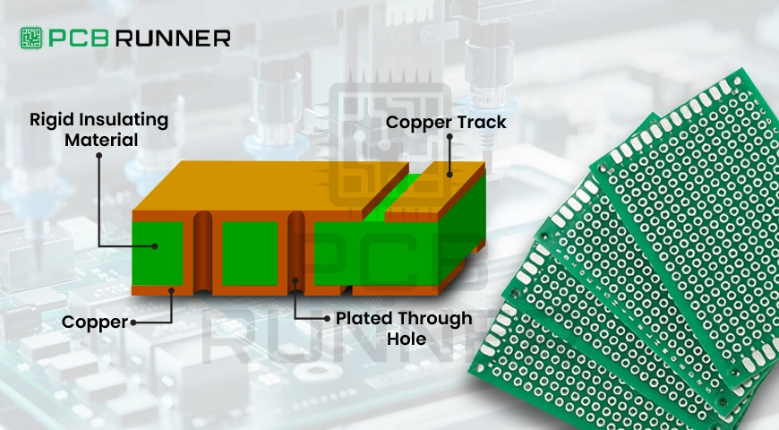
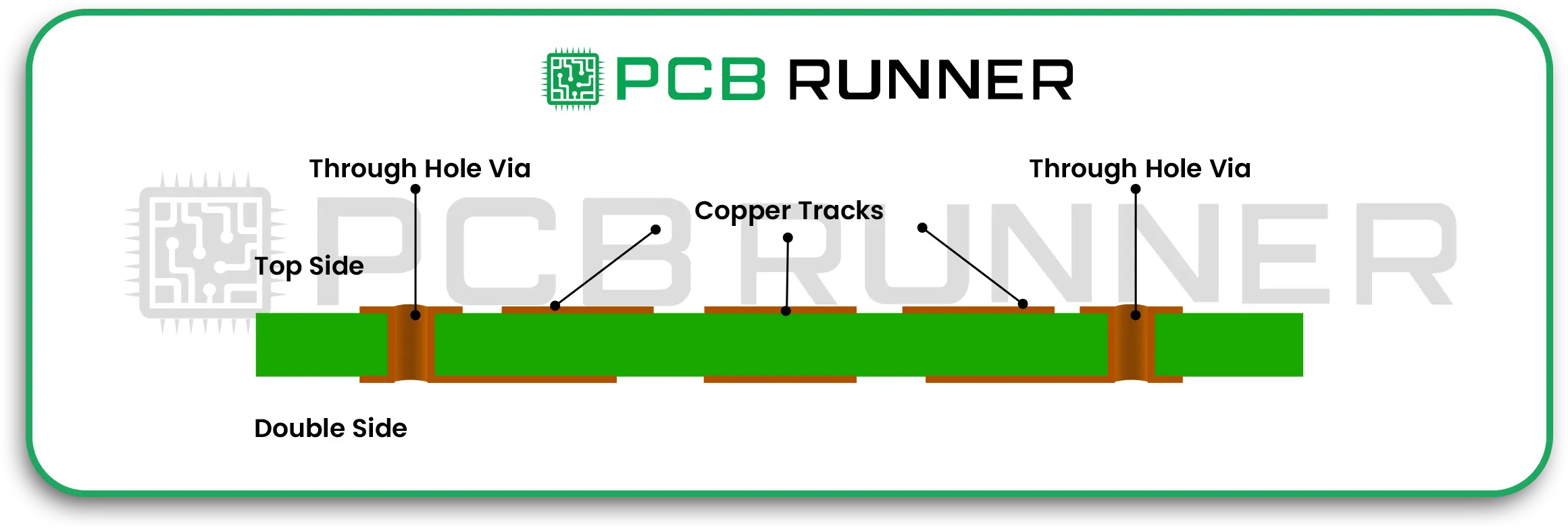
A double-sided prototype PCB is a type of prototype PCB that has copper pads and traces on the top and bottom sides. With this prototype, engineers and designers can connect components on two layers instead of one.
Now, why is that significant? Let’s visualise that you are building a model city. If you can only place roads on the ground (single-sided), you might quickly run out of space and options. If you can add an overpass (double-sided), you can now have more cars and creativity flow. That is the exact benefit that we have here.
How Double-Sided PCBs Are Made
Curious to find out the steps involved in double-sided prototype PCB creation? This is how it looks in a nutshell:
Every board begins with a digital sketch. The first step is laying out all connections which need to be done in advance for a practical layout.
- Choosing Materials: The insulating base (generally FR-4) is sandwiched between copper sheets.
- Drilling: The upper and lower layers can be connected through small holes, which can be likened to little elevators or tunnels.
- Plating Through Holes: During prototype and PCB fabrication, metal is added inside the holes. This provides both sides with an electrical connection, which enables the transfer of signals and power.
- Etching and Printing: Circuit paths are being etched, and both sides of the board can be printed with their respective patterns.
- Adding Solder Mask and Silkscreen: Protective layers are added to the board while simultaneously labelling the critical components.
- Final Testing and Cutting: The boards are checked for accuracy, then cut to shape to the desired dimensions before being dispatched.
Why Use Double-Sided Prototype PCBs?
Imagine for a moment that you are testing electrical circuits for a new device. You’re looking for a space that can accommodate a few chips but not a bulky and multi-layered board. This is where double-sided PCBs shine.
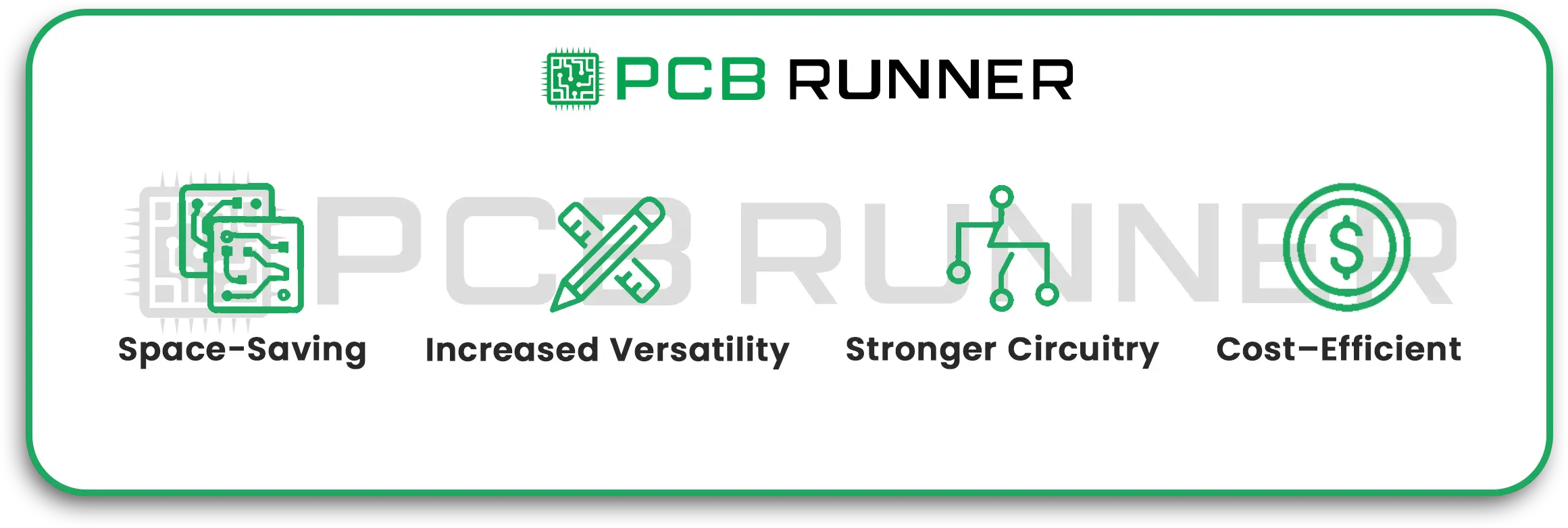
Top Benefits
- Space-Saving: The old saying, “Two Heads are Better Than One,” perfectly captures the use of both sides as components and tracks can be placed on both sides, which is a boon for compact designs.
- Increased Versatility: Excellent for PCB prototype runs and small production batches.
- Stronger Circuitry: More routing flexibility reduces the number of crossed wires, increasing the reliability and sturdiness of the build.
- Cost–Efficient: Fewer cross-sections than multi-layer boards. Less complex than multi-layered boards and more robust than single-sided PCBs.
The Manufacturing Process
Printed circuit board manufacturers work on processes like checking for design match and correctness. Most well-known PCB manufacturers pay special attention to every step while working on double-sided PCBs.
- Verification of the Digital Project: Checking the design against digital files.
- Cutting and Drilling Material: The exact steps, like cutting and shaping materials into boards, and drilling to define thousands of precisely measured holes, are done with the help of CNC machines.
- Through-Hole Copper Plating: The layers are connected with top and bottom “treeshouses” via ladders.
- Soldermask and Circuit Etch: Circuit markings are put on boards to help the device detect malfunctioning components. This is to help decrease the possibility of the device failing.
- Label and Silkscreen: The described steps help to place the PCB in sequential order. The board is “marked” with attention.
Final inspection is done by marking every board for the missing signal paths before assembly. As described, every board is treated the same and pending check for open and shorts.
Marking for every piece is done simultaneously to help with labelling.
Recommendation: Spend less times looking for business needed for prototype designs and order from those who convey up to date step by step processes.
Assembling the Prototype: From Bare Board to Functional Circuit
Board construction begins after a thorough check of the fabrication steps. Turn to PCB Assembly UK Services for the following:
Component Placement: Every chip, resistor, and connector is mounted on the board. This can be Down either by a tiny machine or rather careful hands.
- Soldering: Creating a durable long long-lasting bond. For double-sided boards, the soldering is done on both sides.
- Quality Checking: Every single circuit is visually checked, sometimes using X-ray equipment, to guarantee flawless and perfect connections.
Why Prototypes Matter: Testing Electrical Circuits
No one is perfect, and neither is a device, hence the importance of testing. Prototypes are essential as they help to fine-tune and perfect a design. They are helpful in performing the following:
- Thermal stress, ensuring nothing is overheating or cracking.
- Screaming and checking for open or short-circuits.
- Signal tests.
- Thermal testing.
Prototypes are essential in testing and can save a lot of money when scaling.
Maximising Strategies for Double-Sided Prototyping
Strategically Place Components: Avoid placing sensitive sections near heat and interference.
- Use Labels: Clean labels ensure easier and faster testing and fixing.
- Check for Manufacturer Capabilities: Not all PCB manufacturers have the same features; check for minimum hole size or special materials.
- Don’t wait until it’s done to check; the design should be done as early in the prototype lifecycle to improve wiring or logic changes.
Key Takeaways for Inventors and Makers
- Double-sided prototype PCBs offer a sweet spot of complexity, cost, and flexibility.
- They’re perfect for prototyping, small production runs, and learning new tricks about circuit design.
- Services like pcb assembly uk bring extra value, letting you go from idea to tested device, fast and reliably.
Want a deep dive into double-sided PCB manufacturing? Check this authoritative guide on manufacturing processes.
Conclusion: A Trusted Provider for Double-Sided Prototyping
Double-sided prototype PCBs help realise big ideas in a compact form. They enable engineers, students, and makers to test, refine, and launch innovative electronics in record time. PCB Runner, as one of the leading suppliers, supports advanced fabrication, flexible prototyping, and expert assembly services for the UK and Europe.
When you’re prepared to create, test, and learn, don’t go on a one-sided adventure. Double up and double your opportunities.

