
Impedance can feel like one of those topics that everyone talks about, yet few explain in a simple way. But if you design high-speed circuits, you can’t avoid it. Impedance affects how signals move, how clean they look, and whether your board performs the way you expect. And here’s the thing. Even minor errors in impedance can cause significant problems.
At PCB Runner, we see this a lot. A designer sends a PCB prototype, the build is perfect, but the signals don’t behave the same way they did in simulation. Almost always, the issue comes down to inaccurate impedance values or unclear instructions from the manufacturer.
This guide is here to give you a practical, straightforward way to understand controlled impedance, why it matters, and how to calculate it with confidence.
Introduction to Impedance in PCB Design
Impedance represents how a trace resists changes in current when carrying fast-moving signals. When signals toggle quickly, the trace behaves like a transmission line, not just a piece of copper. This is where impedance becomes essential.
If you work with PCB printing, you already know that copper looks simple on the surface. But electrically, the behaviour is tied to the geometry of the trace and the dielectric material under it.
Your job as a designer is to make sure your traces match the target impedance so your high-speed interfaces run smoothly.
Why Accurate Impedance Control Matters
Accurate impedance helps protect signal integrity. When impedance doesn’t match, signals reflect, lose shape, or distort.
This results in:
- Timing failures
- Data loss
- Higher bit-error rates
- Crosstalk
- Unstable links
That’s why most modern interfaces require controlled impedance. If your impedance is wrong, the signal simply won’t behave as intended.
Fundamentals of Transmission Line Theory
A transmission line carries signals with specific electrical characteristics. A PCB trace becomes a transmission line when:
- Frequency is high
- Rise time is fast
- Signal length is long
Once this happens, the trace has a measurable impedance. Your design must match the expected value.
Types of Transmission Lines in PCBs
There are two main types:
- Microstrip
- Trace on the outer layer with air above and dielectric below.
- Stripline
- Trace sandwiched between two reference planes in the inner layers.
Each behaves differently. Each needs its own impedance calculation method.
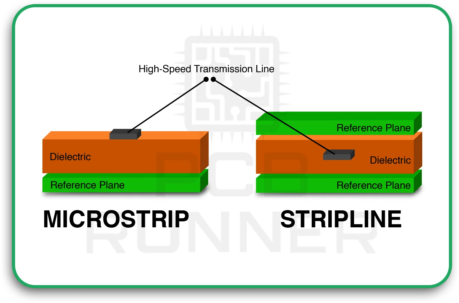
Microstrip vs Stripline Impedance Structures
Microstrip impedance is easier to calculate because part of the electromagnetic field sits in the air. The stripline is more controlled because everything is inside the dielectric.
If you’re working with PCB prototype designs, microstrips appear more often on simple boards. High-speed cores use striplines for tighter signal integrity.
Differential vs Single-Ended Impedance
Single-ended impedance uses a single trace. Differential impedance uses a pair of traces working together.
Differential pairs require:
- Consistent spacing
- Equal length
- Equal geometry
These pairs carry many modern standards like USB, HDMI, PCIe, and DDR.
Key Parameters That Affect Impedance
Impedance depends on the physical details of the PCB. The main factors include:
- Trace width
- Trace thickness
- Dielectric constant
- Distance to reference plane
- Copper roughness
- Solder mask coverage
A slight change in one of these values can shift impedance significantly.
Role of Dielectric Constant (Dk) and Dissipation Factor (Df)
The dielectric constant controls how electric fields propagate. A higher Dk reduces impedance. A lower Dk increases it.
Manufacturers have variations in Dk from sheet to sheet. If you work with printed circuit board manufacturers in the UK, they can tell you the exact Dk values they use in production.
The dissipation factor affects signal loss, not impedance calculation, but it still plays a role in overall performance.
Impact of Trace Width, Thickness, and Spacing
Wider traces have lower impedance. Narrower traces have higher impedance.
Spacing matters most for differential pairs. If spacing changes, the differential impedance shifts.
For controlled impedance, the fabricator adjusts the trace width slightly to hit your target value. You must tell them the exact requirement.
Copper Roughness and Its Effect on Impedance
Copper roughness adds tiny bumps to the surface. These bumps increase the effective dielectric constant near the trace.
This slightly lowers the impedance. The effect becomes more noticeable at higher frequencies.
Core vs Prepreg Material Variations
Core material is more stable. Prepreg changes thickness during lamination.
If your stackup relies heavily on prepreg thickness, the real-world impedance may shift.
This is why you should always provide a complete stackup, not just trace widths.
Accurate Stackup Design for Impedance Control
Your stackup defines:
- Dielectric thickness
- Material type
- Copper weight
- Number of layers
- Reference planes
When the stackup is unclear, impedance cannot be calculated correctly.
Your manufacturer needs stackup details before building your PCB prototype.
Using Field Solvers for Impedance Calculation
Field solvers calculate impedance based on electromagnetic behaviour, not simple formulas.
They are far more accurate because they consider:
- Real Dk values
- Copper roughness
- Solder mask presence
- Fringing fields
- Trace shape
Field solvers reduce guesswork and improve controlled impedance accuracy.
Common Impedance Calculation Models
If you can’t use a solver, these models exist:
- Hammerstad
- Wheeler
- IPC-2141
- Kirschning formulations
They are suitable for approximation but not perfect for production work.
Understanding Impedance Tolerance and Manufacturing Limits
Impedance can never be exact. It comes with a tolerance, usually ±10 per cent.
If you need a tighter tolerance, manufacturing becomes more expensive and more complex.
Effects of Solder Mask on Impedance
Solder mask lowers impedance slightly because it traps more electric field around the trace.
This effect is more potent on microstrip traces than on stripline.
If you want precise numbers, tell CAM whether the trace is covered or not.
Controlled Impedance Requirements for High-Speed Interfaces
Standards that depend on signal integrity include:
- PCIe
- USB
- HDMI
- DDR
- Ethernet
- LVDS
Each one demands a specific impedance value. For example:
- USB: 90 ohms differential
- PCIe: 85 ohms differential
- HDMI: 100 ohms differential
If you’re wrong, the link may fail.
High-Speed Signals: PCIe, USB, DDR, HDMI Considerations
Each interface has a different sensitivity:
- PCIe demands tight length matching
- DDR needs a correct setup and hold timing
- HDMI is sensitive to crosstalk
- USB struggles with reflections
Impedance is the foundation for signal performance.
Differential Pair Routing Guidelines
To maintain impedance:
- Keep spacing constant
- Avoid sudden bends
- Match lengths
- Avoid splitting reference planes
- Don’t allow skew
A small spacing change can shift the differential impedance significantly.
Length Matching and Skew Management
Signals in a differential pair must arrive at the same time. If not, skew happens.
Skew increases jitter and reduces link stability.
Length matching is one of the simplest ways to improve signal integrity.
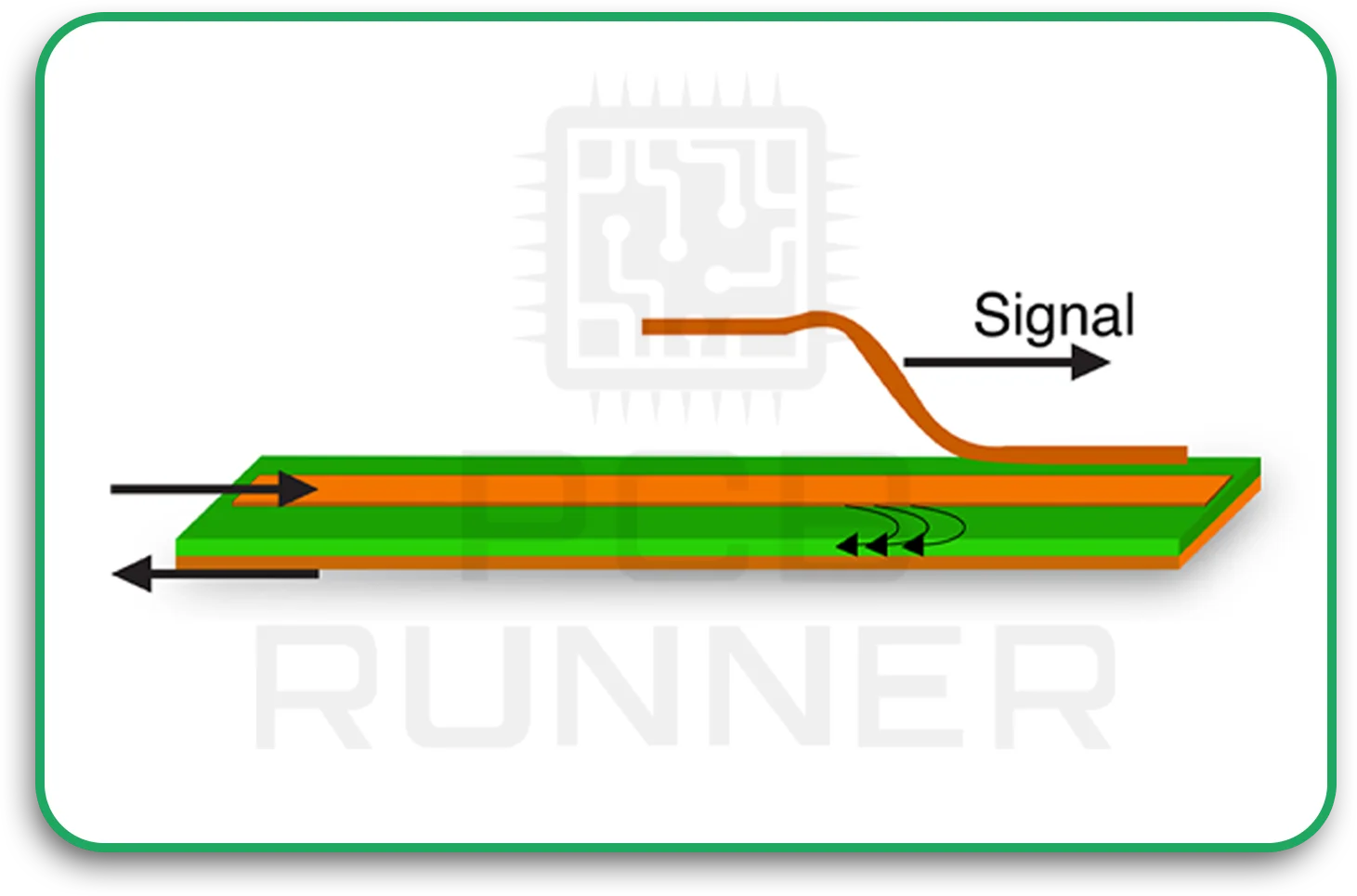
Via Structures and Their Impact on Impedance
Vias add capacitance. They cause small impedance dips. If many vias exist along a high-speed path, they must be modelled.
Backdrilling helps remove unused via stubs, which improves performance.
Return Path Integrity and Reference Plane Usage
Your return path must stay continuous. If the reference plane is cut or missing, impedance jumps and reflections occur.
This is one of the most common pcb layout mistakes.
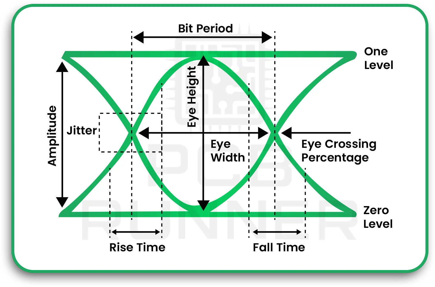
Testing and Measurement Techniques for Impedance
Manufacturers measure impedance using TDR.
TDR (Time Domain Reflectometry) Basics
TDR sends a fast pulse through the trace and measures reflections.
It shows:
- Impedance value
- Impedance changes along the trace
- Discontinuities
- Via effects
It’s the most common testing tool for controlled impedance validation.
Working with PCB Manufacturers for Impedance Validation
When working with printed circuit board manufacturers UK, always:
- Share target impedance
- Share the stackup
- Share trace widths and spacing
- Confirm tolerance
- Review their calculations
Never assume they will guess your requirements.
Common Mistakes in Impedance Design
Mistakes include:
- Missing stackup details
- Forgetting the solder mask effect
- Using formulas instead of solvers
- Splitting reference planes
- Wrong trace spacing
- Incorrect differential routing
Most failures relate to missing information, not bad math.
Also read: Top PCB Assembly Mistakes and How to Avoid Them
How to Document Impedance Requirements in Gerber/ODB++
Include:
- Target values
- Single-ended and differential numbers
- Layer information
- Trace width
- Spacing
- Tolerance
- Type for e.g (coplanar waiveguide) etc.
A simple “controlled impedance” note is not enough.
Cost Implications of Impedance-Controlled PCBs
Expect higher costs because:
- The manufacturer uses tighter process control
- Material consistency must be better
- Testing time increases
Your PCB printing process becomes more specialised.
Best Practices for Reliable Impedance Design
You can avoid headaches by following these rules:
- Use real stackup data
- Use field solvers when possible
- Keep planes continuous
- Match differential lengths
- Keep spacing consistent
- Document everything clearly
These small steps protect your signal integrity.
Future Trends in Impedance Modelling and High-Speed PCB Design
Trends include:
- AI-based modeling
- More accurate material databases
- Advanced solvers for 3D geometry
- Lower-loss dielectrics
- High-frequency optimisation tools
As speeds climb, impedance accuracy becomes even more critical.
Conclusion
Impedance control is one of the foundations of high-speed design. When you understand the factors that influence impedance, you can create boards that behave exactly as intended. With careful stackup planning, good modelling, and clear communication with your manufacturer, your designs will be stable and reliable. And with guidance from teams like PCB Runner, you can handle controlled impedance confidently across all your PCB prototype or production builds.
FAQs
What affects controlled impedance in PCB printing
Controlled impedance in PCB printing is influenced by trace width, dielectric thickness, copper height, and material Dk. All these must be controlled to protect signal integrity.
How do printed circuit board manufacturers UK measure impedance
Printed circuit board manufacturers UK measure impedance using TDR. This validates controlled impedance and checks whether the PCB prototype matches the design.
Why does a PCB prototype need controlled impedance for signal integrity?
A PCB prototype needs controlled impedance to keep reflections low and preserve signal integrity, especially on high-speed interfaces like USB, PCIe, and HDMI.
What parameters matter most for accurate impedance in PCB printing
Trace width, dielectric thickness, copper roughness, and spacing are the main parameters that affect controlled impedance in PCB printing.
Do printed circuit board manufacturers UK help calculate controlled impedance?
Yes. Most printed circuit board manufacturers UK use field solvers to verify controlled impedance values before building the PCB prototype to ensure signal integrity.

