In today’s fast-moving electronics industry, printed circuit board manufacturers are under constant pressure to deliver reliable, high-yield boards at low cost. However, one recurring challenge faced during assembly is the tombstone defect in PCB.This soldering issue can derail production schedules, increase rework costs, and impact overall board reliability.
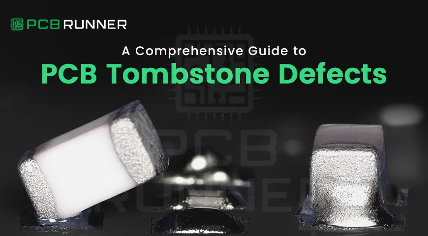
When working on a pcb prototype, even a minor soldering problem can create delays in product launches. The tombstone effect occurs when a small surface-mounted component, usually a chip resistor or capacitor, stands upright during soldering instead of lying flat across both pads. The result is an open circuit that disrupts functionality.
This comprehensive blog will help you to explore what tombstone defect is, how it occurs, why it matters and most importantly what are the best practices and strategies to prevent this.
What is the Tombstone Defect in PCB Assembly?
Understanding the Tombstone Effect and Its Impact
The tombstone defect, also called the tombstone effect, is a common problem during surface-mount technology (SMT) assembly. It often happens with small passive components like 0402 or 0603 resistors. During the reflow process, instead of both ends soldering properly to their pads, one end lifts up, creating an open connection.
For customers and engineers, this defect translates to reduced product reliability, potential field failures, and costly repair work.
Why Tombstone Soldering Defect Matters for PCB Circuit Board Manufacturers
For pcb circuit board manufacturers, yield loss due to the tombstone soldering defect directly impacts profitability. A single defect may not be critical, but on large production runs, small percentages add up. For pcb prototype builds, the defect delays validation and forces redesigns or rework, consuming valuable engineering resources.
Causes and Mechanisms Behind Tombstone Defects
Imbalanced Solder Wetting and Surface Tension Forces
The tombstone effect often stems from uneven solder wetting. If one pad reaches the solder reflow temperature faster than the other, molten solder pulls the component upright. This imbalance in surface tension is the root mechanical driver of tombstoning.
PCB Prototype Design, Pad Layout, and Thermal Gradients
Poor PCB prototype design decisions like using pads of different sizes or not following the pad dimensions according to the component datasheet. This can also happen by keeping uneven copper surface for heat to spread unevenly across the board. During reflow, one side of a component may heat up faster than the other, increasing the chances of tombstoning.
At PCBrunner, our engineering team uses advanced DFM & DFA analysis and controlled reflow profiling to prevent defects like tombstoning before they occur. Whether you’re developing prototypes or scaling to full production, our end-to-end PCB assembly services guarantee precision and yield reliability.
Solder Paste Properties and Component Geometry
Incorrect solder paste volume or stencil design can also cause tombstoning. Too little solder on one side or variations in paste thickness create uneven forces. Similarly, very small components are more susceptible due to their light weight and reduced contact area.
Solutions and Strategies to Prevent Tombstone Defects
Best Practices in PCB Prototype Layout and Pad Design
Careful layout is the first line of defense. Printed circuit board designers should follow:
- Keep pad dimensions symmetrical.
- Balance copper distribution around pads.
- Use proven land pattern standards such as IPC-7351.
For pcb prototypes, correcting pad design early prevents recurring tombstone defects in scaled-up production.
Process Control: Solder Paste, Reflow, and Placement Accuracy
Precise solder paste application is critical. Strategies include:
- Using high-quality solder paste with consistent viscosity.
- Verifying stencil aperture height, design and alignment.
- Ensuring accurate component placement with modern pick-and-place machines.
- Optimizing reflow profiles to minimize temperature imbalances.
Using Anti-Tombstone Materials and Alloys
Some printed circuit board manufacturers reduce tombstoning by adopting low-tombstone solder alloys. Nitrogen atmosphere reflow is another technique that helps stabilize wetting and reduces soldering defects.
Real-World Examples and Best Practices from PCB Circuit Board Manufacturers
Lessons from PCB Prototype Runs
When building a pcb prototype, engineers often discover tombstone defects during early testing. For example, a consumer electronics manufacturer identified recurring tombstoning in their prototype due to uneven copper surfaces between component pads, which then they eliminate by making revision of design before mass production saving thousands in potential rework.
Industry Standards and Case Studies
Adopting IPC standards for pad design, solder paste deposition, and reflow process validation is a proven best practice. Case studies across industries show that collaboration between design engineers and pcb circuit board manufacturers leads to significant yield improvements and fewer tombstone defects.
Common Mistakes and FAQs About Tombstone Defects
Misunderstanding the Root Cause
Many teams assume the tombstone defect in PCB is purely a process issue. In reality, it is often a combination of layout, materials, and process control. Overlooking design factors while only tweaking reflow settings may not solve the problem.
Overlooking PCB Prototype Testing
Another common mistake is underestimating the value of thorough pcb prototype testing. Early detection of tombstone soldering defects allows manufacturers to refine both design and assembly processes before scaling up. Skipping this step increases risks during production.
Conclusion
The tombstone defect in PCB assembly is a persistent challenge, but it is not insurmountable. By understanding the mechanisms that cause tombstoning and adopting proven preventive strategies, pcb circuit board manufacturers can improve yields, lower costs, and deliver more reliable products.
For teams developing a pcb prototype, early focus on design symmetry, solder paste application, and reflow control ensures fewer defects when moving to mass production.
Are you looking to eliminate tombstone defects and improve assembly reliability? Contact our experts today to learn how our advanced pcb circuit board manufacturing solutions and prototyping services can support your upcoming project.

