When you start working with high-frequency signals, a PCB stops being just copper and fiberglass. It starts behaving like a real electrical environment where fields, noise, and tiny layout choices can change everything. If you’ve ever wondered why a board looks perfect on-screen but fails during testing, high-frequency behaviour is usually the reason.
At PCB Runner, we often see designers create clean layouts that still run into trouble once the board is powered. And the truth is simple. High-frequency signals don’t follow the rules you learned when you first started designing. They follow physics, not your drawing tools.
Let’s break this topic down so you understand what really happens at high frequencies and how to design for it with confidence.
Introduction to High-Frequency PCB Design
When signals move slowly, the PCB doesn’t care much about trace shape, spacing, or return paths. But once the frequencies rise, everything becomes sensitive. Traces act like transmission lines. The ground plane becomes your signal partner. Even a small via starts influencing performance.
If your work involves PCB production UK or any project that ends up going through PCB assembly services, learning how high-frequency behaviour works will help you avoid painful redesigns.
What Counts as High Frequency in PCB Systems
High frequency doesn’t have a single number. What really matters is how fast the signal rises. A simple rule helps:
If the trace length is longer than about one-tenth of the signal’s wavelength, you’re in high-frequency territory.
Digital designs often reach this point around a few hundred MHz. RF designs reach it much earlier.
Electromagnetic Behaviour at High Frequencies
Here’s what changes. Signals stop behaving like simple currents. They travel as electromagnetic fields around the trace. The shape of the copper, the material under it, and even the air above it all affect performance.
This is why two traces that look identical can behave differently once frequency goes up.
Signal Integrity Challenges at High Speed
Fast signals bring new challenges you may not notice at lower speeds:
- Reflections
- Noise that jumps between traces
- Distorted waveforms
- Timing shifts
- Data errors
These fall under signal integrity, and fixing them usually starts with layout choices.
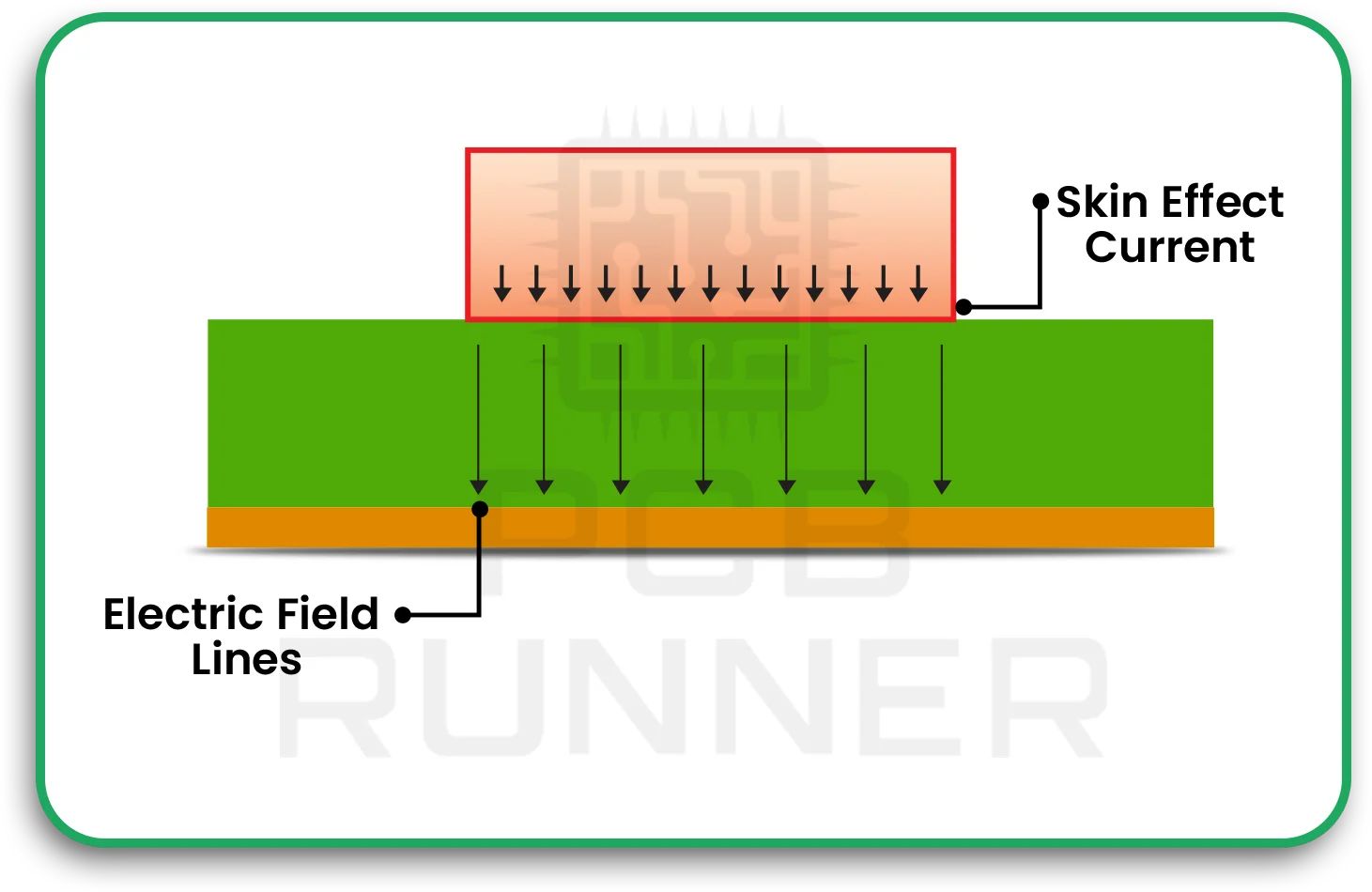
Skin Effect and Its Impact on Trace Resistance
The skin effect forces high-frequency current to flow only on the outer surface of a trace. That means resistance increases as frequency goes up.
More resistance creates more heat and more signal loss. You can’t eliminate the skin effect, but you can design knowing it exists.
Dielectric Losses and Material Considerations
Every PCB material absorbs some energy. At high frequencies, this becomes a bigger problem. FR-4 may be fine for moderate speeds, but RF designs often need materials with lower loss.
If your design relies on high-speed routing, the choice of dielectric can make or break your final performance.
Conductor Geometry and High-Frequency Loss
Trace width, height, and shape all influence how the signal behaves. Narrow traces lose more energy. Wide traces raise capacitance. Sharp corners cause reflections.
What this really means is that high-frequency geometry is never “just a trace.” It’s part of the signal path with its own electrical weight.
Impedance Control Requirements
High-frequency traces must hold a stable impedance. If the impedance suddenly changes, the signal reflects back. This reflection can ruin data timing or create unnecessary noise.
Manufacturers working in PCB production UK may adjust your trace width slightly to hit the exact impedance you requested.
Crosstalk Mechanisms in High-Frequency Designs
High-frequency fields spread sideways. If two traces run too close for too long, the energy couples between them. That’s crosstalk.
You’ll see more crosstalk when:
- Traces run in parallel
- There is no solid ground plane
- Spacing is inconsistent
- Differential pairs aren’t balanced
Good spacing rules reduce most of this.
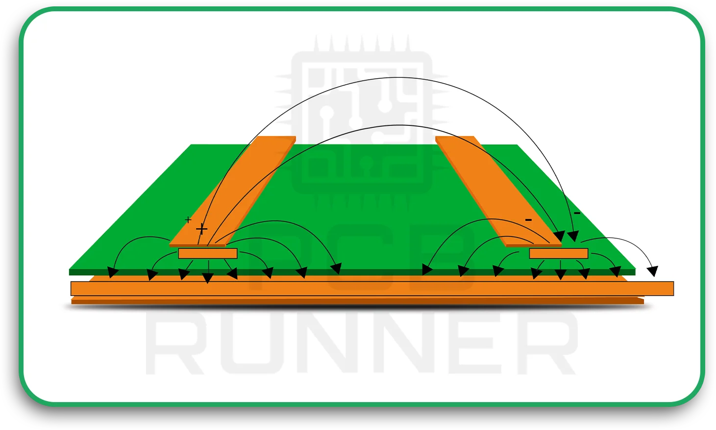
Return Current Path at High Frequencies
Return current isn’t random. It follows the path of least impedance, not the path of least resistance. That usually means it sits right under the trace on the reference plane.
If that plane has gaps or splits, the return current takes a detour. That detour increases noise and radiation.
Ground Plane Strategies for High-Frequency PCBs
A good ground plane solves many high-frequency problems. It gives signals a clean return path, reduces EMI, and stabilises impedance.
Use solid planes whenever you can. When you need to switch layers, use stitching vias to keep the return flow tight.
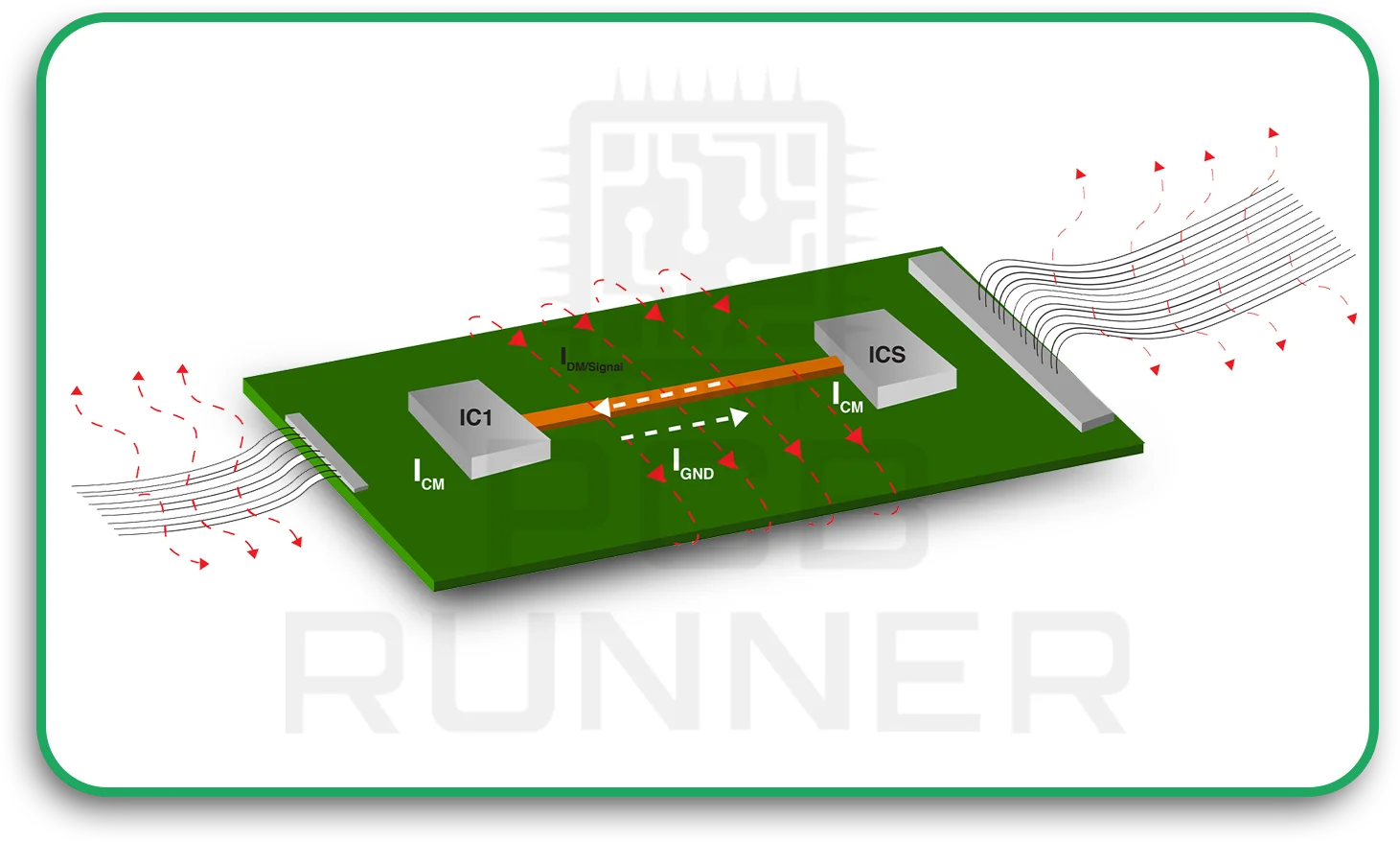
High-Frequency Noise and EMI/EMC Performance
As frequency goes up, radiation becomes stronger. Even a simple layout mistake can create a significant EMI problem.
Poor EMI/EMC performance usually comes from:
- Long current loops
- Disrupted ground planes
- Poor filtering
- Sharp corners
- Bad shielding
Small improvements in layout often reduce EMI dramatically.
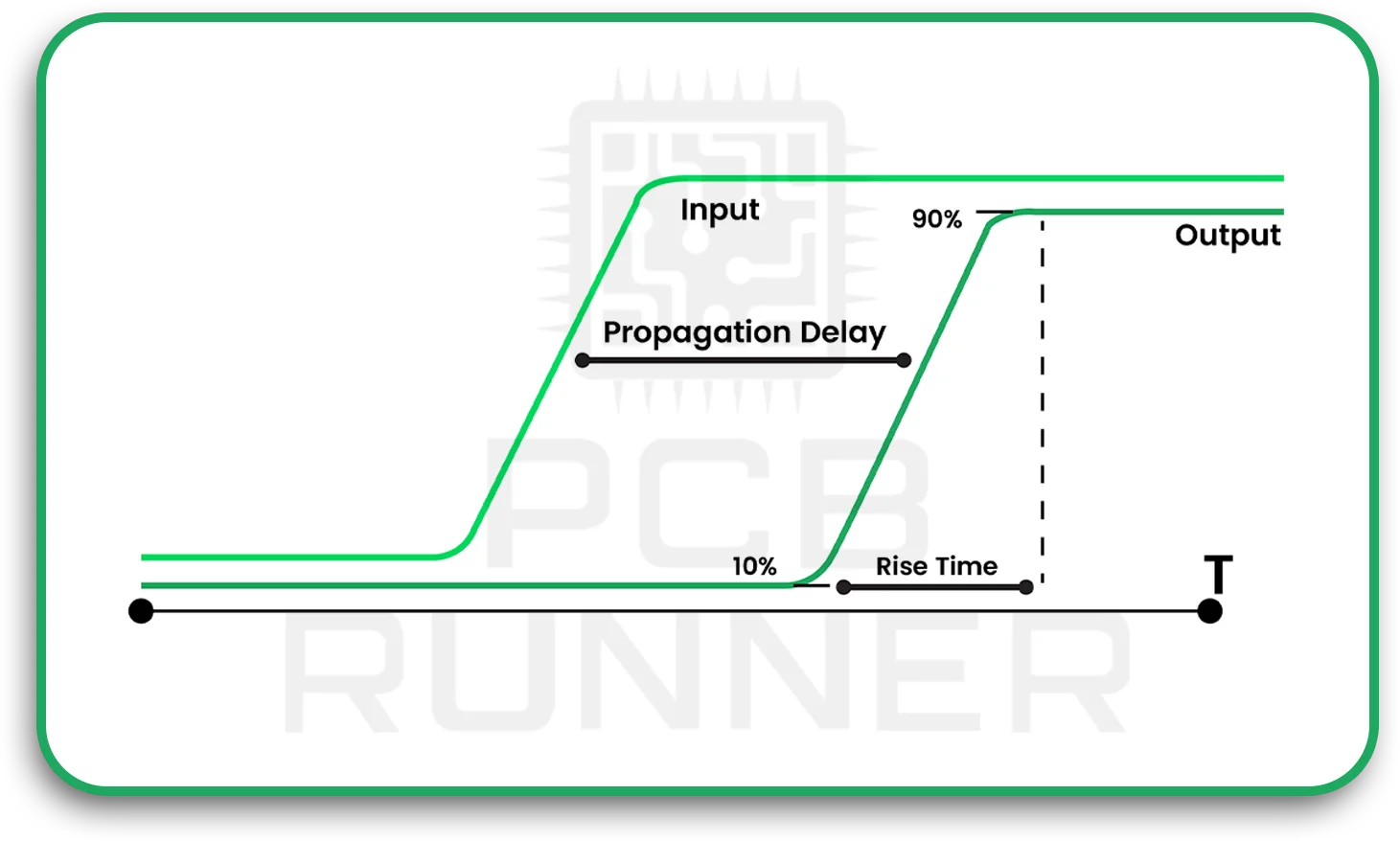
Managing Reflections and Signal Discontinuities
Reflections happen whenever the signal sees a sudden change. This can occur at:
- A via
- A connector
- A trace width change
- A plane gap
- A stub
The cleaner your path, the fewer reflections you’ll see.
Effects of Vias and Transitions on High-Speed Signals
Vias add inductance. They also create a slight change in impedance. One via isn’t a problem. A chain of vias can be.
If your frequency is high enough, backdrilling removes unused via stubs and keeps your path clean.
Routing Techniques for High-Frequency Signals
Here’s a simple guide for high-frequency routing:
- Keep traces short
- Avoid sharp corners
- Stick to one layer when possible
- Keep spacing consistent
- Maintain a steady reference plane
Every decision matters at high speed.
Differential Pair Routing Considerations
Many high-frequency standards use differential pairs. They only work well when both traces are equal.
Keep:
- Lengths matched
- Spacing consistent
- Widths equal
- Both are on the same layer
An uneven pair loses its noise-cancelling ability.
Stackup Design for High-Frequency Performance
A well-designed stackup often fixes more problems than any routing tweak. Good stackups use:
- Solid ground planes
- Predictable dielectric thickness
- Controlled impedance layers
- Defined separation for differential pairs
If you’re preparing a board for PCB assembly services, share your stackup early. It avoids mistakes later.
Role of Copper Roughness in High-Speed Loss
Copper roughness increases the path length of the signal. That adds loss. At high frequencies, this becomes more noticeable.
Smooth copper helps reduce this problem.
Decoupling and Power Integrity Challenges
Fast signals need clean power. Noise on the power plane can show up on high-speed lines.
Use:
- Short decoupling paths
- Multiple capacitor values
- Tight placement near IC pins
Good power integrity supports good signal integrity.
PCB Material Selection for RF and High-Speed Designs
Not all materials behave the same. If your frequencies are high, consider:
- PTFE
- Low-loss laminates
- Stable Dk materials
Standard FR-4 may distort signals at very high speeds.
High-Frequency Component Placement Guidelines
Good layouts start with good placement.
Try to:
- Keep high-speed paths short
- Place connectors near their controllers
- Avoid routing under noisy power circuits
- Group RF parts together
Placement mistakes are hard to fix later.
Transmission Line Behaviour in PCB Routing
At high frequencies, every trace becomes a transmission line. That means:
- Length matters
- Width matters
- Impedance matters
Understanding this idea makes routing choices much simpler.
Filtering and Termination Techniques
Proper termination reduces reflections. Filtering reduces noise.
You’ll often use:
- Series resistors
- AC coupling caps
- Common-mode chokes
- End-terminating resistors
These small parts play a significant role in stability.
Design Rules for RF and Microwave PCB Layers
RF layers follow stringent rules:
- Avoid unnecessary vias
- Control impedance
- Use full ground planes
- Keep spacing predictable
- Minimise stubs
Many printed circuit board manufacturers in the UK offer RF-specific guidance if you need help.
Thermal Management at High Frequencies
High-frequency circuits generate heat. Power amplifiers and mixers are especially sensitive.
Use:
- Thermal vias
- Thick copper in power areas
- Heat spreaders
- Balanced copper distribution
Good thermal design protects performance.
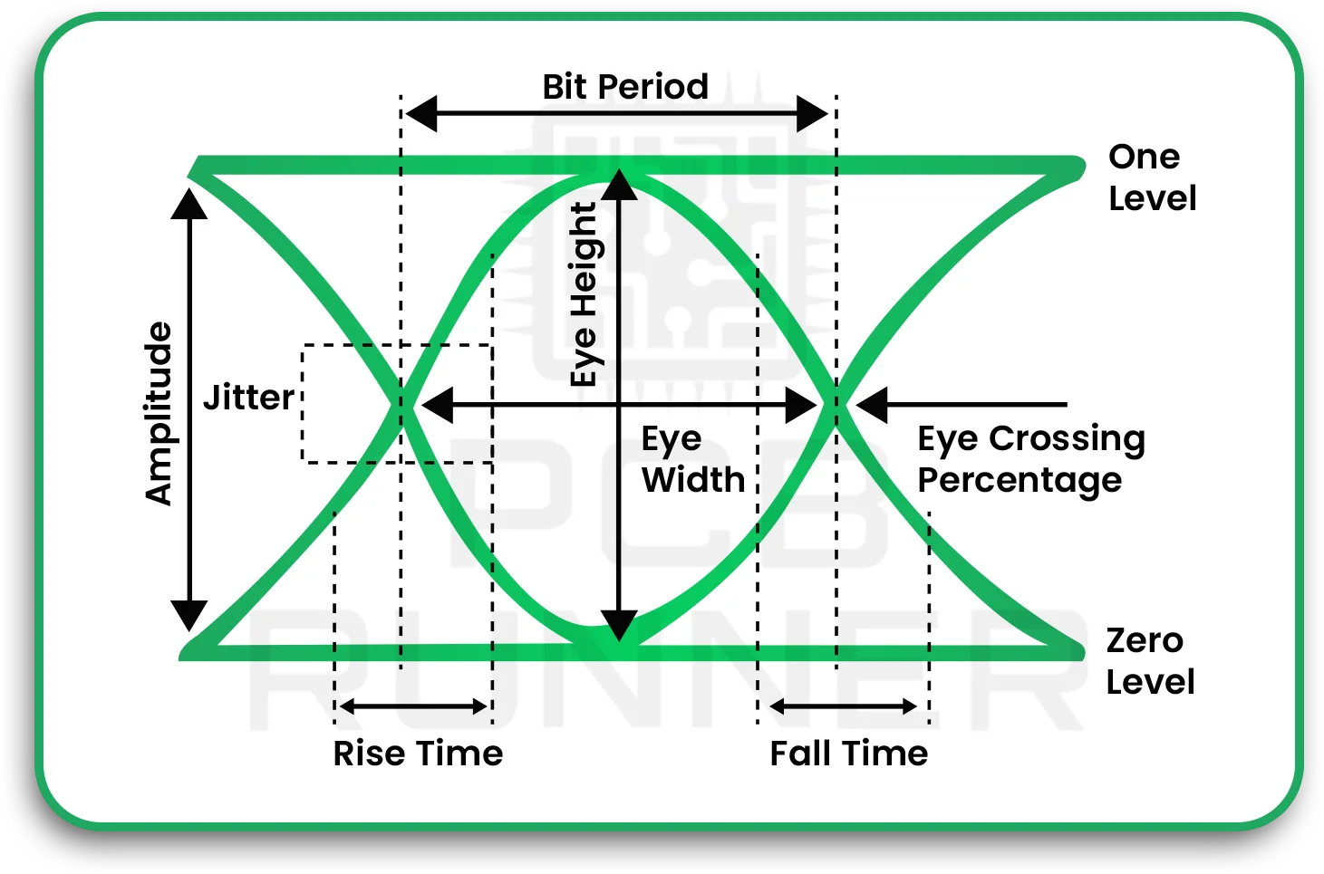
Testing and Validation for High-Frequency PCBs
You cannot rely on simulation alone. High-frequency boards need testing.
Common methods include:
- TDR for impedance
- VNA for frequency response
- Spectrum analysers for EMI
- Oscilloscope eye diagrams
Testing shows what the real PCB does, not what the model assumed.
Common Mistakes in High-Frequency PCB Layout
Mistakes to avoid:
- Long parallel traces
- Splitting the ground plane
- Poor stackup planning
- Missing decoupling
- Excessive use of vias
- Tight spacing without reason
Most problems come from not planning early enough.
Working with Manufacturers for High-Frequency Builds
Manufacturers need clear instructions. When working on PCB production UK or with complete turnkey assembly, share:
- Stackup
- Material choices
- Impedance targets
- Pair spacing
- Length-matching rules
Clear documentation reduces errors.
Best Practices for Reliable High-Frequency PCB Design
If you want consistent results:
- Keep reference planes solid
- Match differential pairs well
- Use smooth, short traces
- Choose materials carefully
- Document everything clearly
- Test early
These habits make high-frequency work much easier.
Future Trends in High-Speed and RF PCB Technologies
Expect more:
- Lower-loss materials
- Integrated RF structures
- Smaller wavelengths
- Higher data rates
- Boards that combine RF and digital sections
Your layouts will need to adapt as frequencies rise.
Conclusion
High-frequency design is all about understanding how signals move and how the layout shapes their behaviour. When you learn how fields, noise, and materials interact, you gain control over your design. With careful planning and clear communication with your manufacturers or PCB Runner, you can create boards that handle high speeds, noise, and demanding environments with confidence.
FAQs
How does high-speed routing affect EMI/EMC performance in PCB production in the UK?
High-speed routing changes how signals radiate. This affects EMI/EMC performance during PCB production in the UK because fast edges generate stronger noise fields that must be controlled through good layout and grounding.
Why do PCB assembly services care about high-frequency layout choices?
High-frequency layouts require proper stackups, spacing, and impedance. PCB assembly services work best when these details are precise, so the final build supports stable signal flow.
Can poor layout cause a PCB prototype to fail EMI/EMC performance tests
Yes. A PCB prototype can fail tests when layout mistakes increase noise or reflections. This reduces EMI/EMC performance and may require redesign.
Do printed circuit board manufacturers UK support high-speed routing for RF boards
Most printed circuit board manufacturers UK offer stackup options, materials, and advice that help with high-speed routing and controlled impedance.
Why is signal integrity important during complete turnkey assembly
During complete turnkey assembly, components rely on clean signal paths. Good signal integrity helps the full board meet timing, noise, and interface requirements.

