Designing a printed circuit board is not just about drawing traces and placing components footprints. What really determines whether your design will build correctly is the connection between your CAD work and how the CAM team interprets it. If these two sides don’t match, even small mistakes can turn into delays, scrap, or failed tests.
At PCB Runner, we see this gap often.Designers prioritize the design layout based on the netlist checks, however PCB CAM engineers have other manufacturing based observations in the designs. When both sides understand each other, the entire PCB fabrication assembly process becomes smoother, cheaper, and more predictable.
Let’s break it down in a way that shows you what actually improves build quality and how you can prevent errors before they ever reach the shop floor.
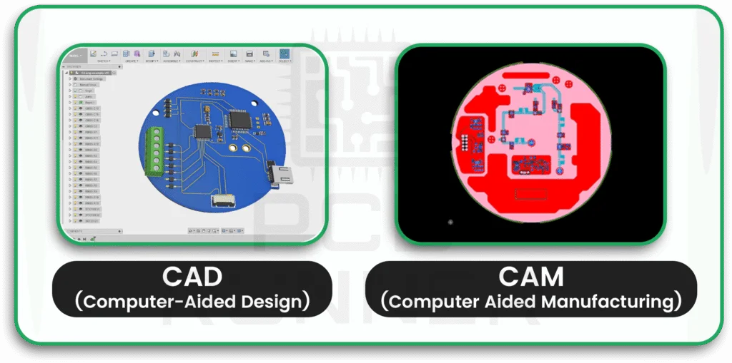
Introduction to CAD and CAM Collaboration in PCB Design
CAD tools are built for designing. CAM tools are built for manufacturing. Both sides depend on the same data, but they interpret it differently.
If you design custom printed circuit board layouts, you already know how many details must line up, stackups, tolerances, drill sizes, copper weights, clearances, and more. When this information is not communicated clearly, your manufacturer spends extra time guessing your intent. This is a common source of delays.
The goal is simple. Your CAD data should tell the CAM team exactly what you expect. No assumptions.
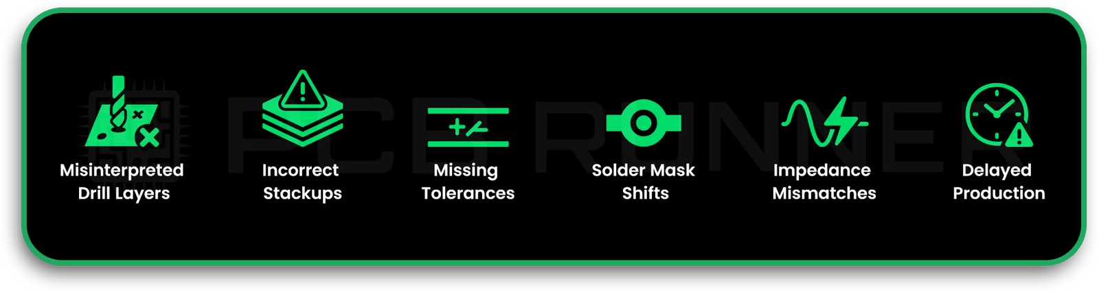
Why CAD-CAM Alignment Matters in Modern PCB Manufacturing
Here’s what this really means for you. When CAD and CAM match, you avoid:
- Misinterpreted drill layers
- Incorrect stackups
- Missing tolerances
- Solder mask shifts
- Impedance mismatches
- Delayed production
Modern PCB circuit board manufacturers use automated systems to read your files, but these systems only work when the data is complete and organised.
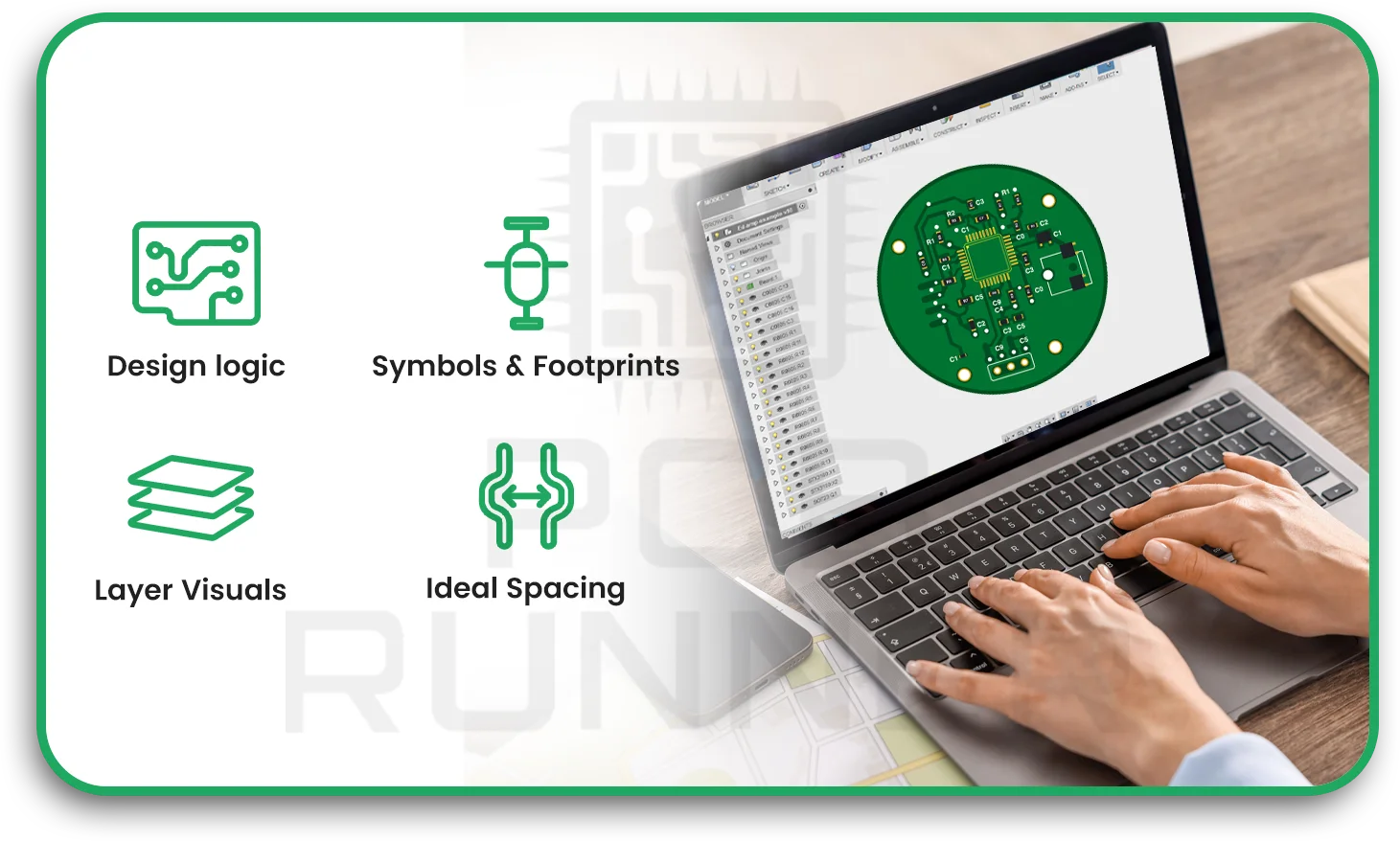
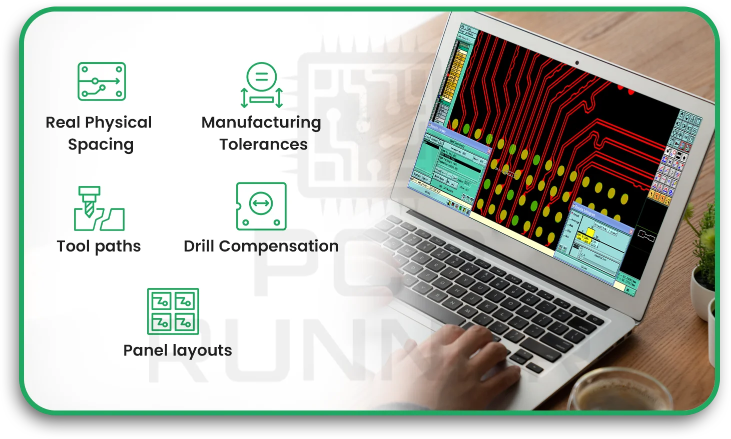
Key Differences Between CAD and CAM Data
CAD data represents your design view. CAM data represents the manufacturing view. These views are not identical.
CAD shows:
- Logical connectivity
- Symbols and footprints
- Layer visuals
- Ideal spacing
CAM shows:
- Real physical spacing
- Manufacturing tolerances
- Tool paths
- Drill compensation
- Panel layouts
You need both perspectives to avoid mismatches.
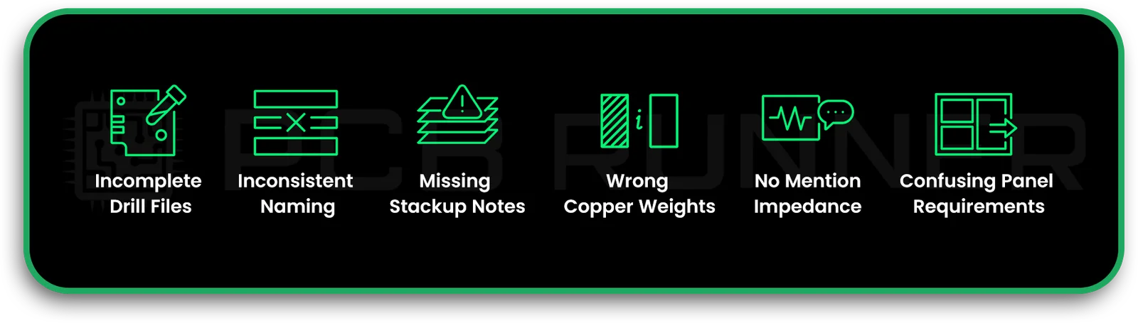
Common Communication Gaps Between Design and Manufacturing Teams
Most problems start with silence. The designer assumes the manufacturer knows the intent. The manufacturer assumes the designer understands the limitations of PCB fabrication and assembly.
Common gaps include:
- Incomplete drill files
- Inconsistent naming
- Missing stackup notes
- Wrong copper weights
- No mention of controlled impedance
- Confusing panel requirements
These issues lead to redraws or production stops.
Understanding DFM, DFA, and DRC Requirements
DFM guidelines help ensure your board can be built without issues. DFA focuses on assembly. DRC checks design rules inside your CAD tool, but that is not enough unless your tool is aligned with your manufacturer’s real capabilities.
If you don’t follow published DFM guidelines, CAM engineers must guess how to repair or modify your data.
Standard File Formats for CAD-to-CAM Transfer
Most PCB circuit board manufacturers accept these formats:
- Gerber RS-274x
- ODB++
- IPC-2581 (Netlist Information)
- Drill and route files (Excellon)
- Pick-and-place files
The more organised your output package is, the faster CAM can start reviewing your job.
Importance of Accurate Manufacturing Data Outputs
Sound CAD output should:
- Include every file needed
- Match naming conventions
- Show consistent polarity
- Contain readable drill tables
A single mislabeled file can hold up an entire production batch.
Layer Stackup Communication and Validation
Your stackup defines everything, impedance, drill depth, plating thickness, and thermal behaviour.
Always share:
- Material type
- Overall board thickness
- Dielectric (Core or prepreg) thickness
- Copper weights
- Any HDI or microvia spans notes
Without this information, it’s hard for the CAM reviewer to validate the design for manufacturing.
Clearance, Spacing, and Tolerance Documentation
CAM engineers use manufacturing tolerances to decide whether a trace, pad, or hole meets capability. When you don’t document these tolerances, the review process slows down.
Provide:
- Min trace width
- Min spacing
- Hole tolerance
- Plating thickness
- Solder mask clearance
Simple notes prevent expensive mistakes.
Handling Drill Files, Vias, and Plating Requirements
Drill files must always match the drill chart in your CAD design. Even a slight mismatch causes confusion in PCB fabrication and assembly.
Include:
- Finished hole size
- Plated vs non-plated
- Aspect ratios
- Backdrill requirements
- Via tenting, plugging, or filling needs
For HDI boards, you must also specify microvia layers clearly.
Communicating Controlled Impedance Requirements
If your PCB needs controlled impedance, do not assume the manufacturer will guess your values. Tell them:
- Target impedance
- Trace width
- Trace height
- Formula used for e.g (coplaner waive guide) etc.
- Tolerance allowed (+/-10%, 7% or 5%)
This helps CAM produce exact working stackup after taking out fudge and etch factors.
Solder Mask and Silkscreen Alignment Issues
Solder mask misalignment is one of the most common issues in manufacturing. CAM needs precise mask data, especially around pads.
Check for:
- Floating pads
- Exposed copper
- Tight mask dams
- Overlapping text
These error looks small but end up showing issues as shorts, unreliable solder due to excessive solder resists on pads spacing or text overlapping.
Copper Weight, Trace Width, and Thermal Relief Considerations
Different copper weights require different trace widths and spacing. CAM engineers adjust their processing for thicker copper, so they must know precisely what copper weight you expect.
For thermal reliefs, give clear instructions for:
- Heat-sensitive parts
- Large copper pours
- Ground and power areas
- Ensure the stackup has sequentially balanced copper weights in every layer for multilayer PCBs.
This helps prevent soldering defects like tombstoning or warpage.
Panelisation Guidelines and Manufacturing Constraints
Panelisation affects fabrication cost and speed. When you don’t specify panel needs, PCB circuit board manufacturers will guess. Sometimes they guess wrong.
Communicate:
- Board orientation
- Tooling holes
- Fiducials
- Break tabs
- V-grooves or routing
The clearer this step is, the smoother your build goes.
Material Specs and Laminates Used in PCB Fabrication
Materials influence signal speed, heat flow, drill quality, and overall durability.
List:
- FR4 type
- High-speed laminates
- Flex or rigid-flex materials
- Tg values
- Loss characteristics
The CAM team uses this to validate your stackup.
Capturing HDI and Microvia Requirements for CAM Accuracy
HDI boards need exact communication. Tell CAM:
- Via types
- Laser via layers
- Sequential lamination notes
- Via filling needs
- Depth control
This information must match your custom printed circuit board instructions.
Ensuring Accurate Component Footprints and Land Patterns
Footprints cause assembly failures when incorrect. Make sure:
- Pad sizes match part datasheets
- Courtyards are correct
- Thermal pads show paste openings
- Polarities are clear
A wrong footprint delays assembly more than anything else.
Version Control and Change Management Across Teams
Design versions change fast. If the CAM team receives the wrong version, the build fails.
Use simple practices:
- Unique version names
- Change logs
- Shared folders
- Locked release packages
This keeps CAD and CAM aligned.
Simulation Data and CAM Interpretation
Simulation helps predict how your board behaves electrically. CAM uses your simulation notes to verify critical areas, such as impedance traces, high-speed pairs, and sensitive nets.
Share:
- Simulation values
- Sensitive nets
- Differential pair details
- Return path concerns
These help CAM flag risks.
Using 3D Models to Improve CAD–CAM Understanding
3D models reduce errors by showing real part heights, clearances, and assembly spacing. CAM teams use 3D models to check shadowing issues and solder access.
Early Manufacturer Involvement in the Design Cycle
The earlier your manufacturer reviews your design, the fewer revisions you’ll need later. Many issues are caught before the layout is finished.
Automated CAD–CAM Validation Tools
Tools that compare CAD files with manufacturing limits can catch:
- Violated clearances
- Wrong holes
- Mask overlaps
- Missing files
They save time and prevent rework.
Feedback Loops and Error Reporting Workflows
A simple feedback loop between CAD and CAM ensures errors get resolved quickly. When CAM reports an issue, update the design and resend only the changed files.
Creating Standardised CAD Output Packages
A clean output package contains:
- Gerbers
- Drill files
- Stackup notes
- Netlist
- Assembly data
- Pick-and-place
- Readme with all instructions
This speeds up PCB fabrication and assembly in any region.
Best Practices for Reducing Fabrication Errors
To reduce errors:
- Follow DFM guidelines
- Double-check footprints
- Send full stackup details
- Use standard layer names
- Validate drill charts
- Confirm mask openings
Small steps make significant differences.
Collaboration Platforms and Digital Thread Integration
Shared platforms keep CAD and CAM synced. A digital thread lets teams follow the entire history of a custom printed circuit board design.
Case Examples of Improved CAD–CAM Coordination
When communication is clear:
- Lead times drop
- Scrap reduces
- Layer mismatches disappear
- Impedance issues get resolved early
These real gains come from a better understanding.
Future Trends in CAD–CAM Collaboration for the PCB Industry
Expect more:
- Cloud-based design platforms
- AI-driven file checking
- 3D simulation tied directly to CAM
- Unified file standards
The goal is more precise data and fewer mistakes.
Conclusion
Clear CAD and CAM communication is one of the most critical steps in building reliable boards. When your files match your intent, manufacturers can produce your custom printed circuit board exactly as expected. With support from teams like PCB Runner, you can reduce fabrication errors and achieve smoother PCB fabrication and assembly across any project.
FAQs
How does CAD CAM integration improve PCB fabrication and assembly?
CAD CAM integration helps manufacturers interpret design data correctly, which improves accuracy in PCB fabrication and assembly and reduces production errors.
Why do PCB circuit board manufacturers need complete DFM guidelines?
PCB circuit board manufacturers need clear DFM guidelines so they can validate spacing, drill sizes, copper weights, and stackups before starting fabrication.
What files are needed for custom printed circuit board production
To build a custom printed circuit board, manufacturers need Gerber, drill files, stackup notes, pick-and-place data, and DFM guidelines that match CAD CAM integration rules.
How do designers reduce mistakes during PCB fabrication and assembly?
Designers reduce mistakes by following DFM guidelines, organising CAD files correctly, and improving CAD CAM integration with their PCB circuit board manufacturers.
Why is CAD CAM integration necessary for impedance control?
Accurate CAD CAM integration helps maintain controlled impedance on a custom printed circuit board, since manufacturers rely on correct stackup and trace details.

