
When you look at your phone, a computer, or even a modern car, you probably don’t think about the tiny highways inside that move information at lightning speed. But those highways, built into printed circuit boards (PCBs), are what make today’s fast, smart devices possible. And now, with optical layers joining the mix, those highways are getting faster and more reliable than ever.
If you’re curious about how optical layers work in PCB manufacture, or you want to know what it means for your next project, you’re in the right place. Let’s break down what makes optical integration so important, how fibre optic printed circuit boards are built, and why this matters for you and your business.
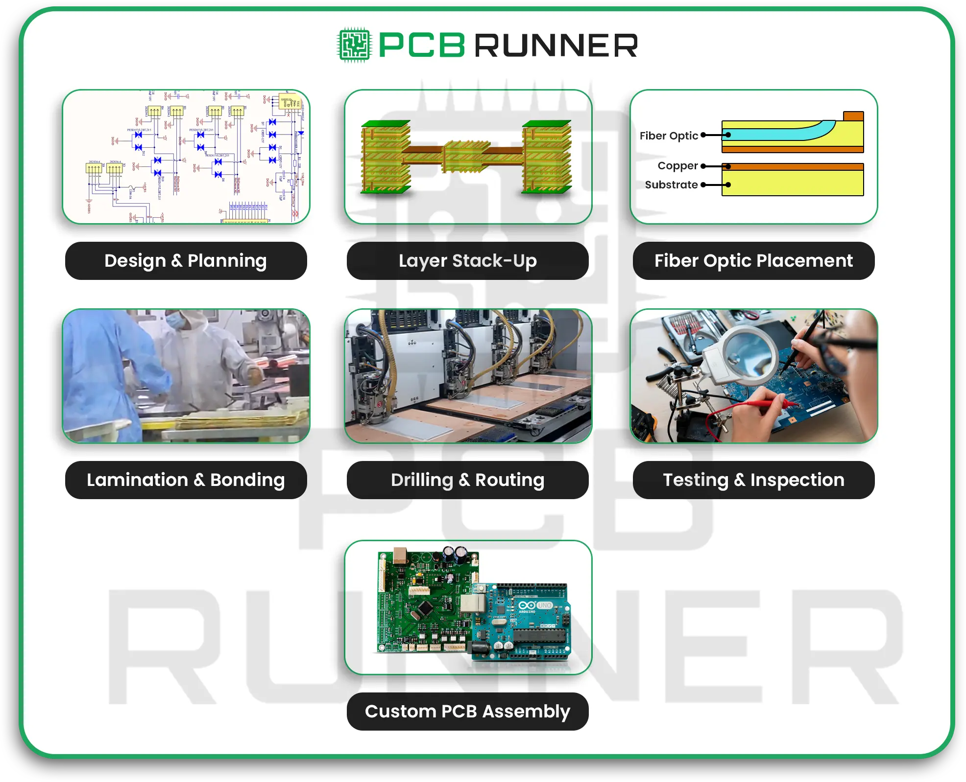
What Are Optical Layers in PCBs?
Traditional PCBs use copper traces to carry signals. These traces are like tiny roads for electricity. But as our need for speed grows, think faster internet, better streaming, and smarter machines, copper sometimes hits its limits. That’s where optical layers come in.
Optical layers use light instead of electricity to move information. Inside the board, you’ll find fibre optic interconnects or special optical channels. These can carry more data faster and with less interference. It’s a bit like swapping out a busy city street for a high-speed train, suddenly, everything moves quicker and smoother.
Why Use Optical Integration PCB Technology?
Let’s keep it simple. Here are the main reasons you might want optical layers in your PCB printed circuit board assembly:
- Speed: Light travels faster than electricity, so you get quicker data movement.
- Bandwidth: Optical interconnects can handle more information at once.
- Less Noise: Optical signals aren’t bothered by electrical interference.
- Distance: Fiber optic interconnects can send signals further without losing quality.
If you’re building telecom equipment, servers, or anything that needs to move lots of data, these benefits are a big deal.

How Optical Layers Fit into PCB Manufacture
Adding optical layers to a PCB isn’t just about sticking in a few extra parts. It’s a careful process that starts at the design stage and goes all the way through custom PCB assembly. Here’s how it usually works:
Design and Planning
First, you and your team decide where you need optical channels. Maybe you want to connect two chips that are far apart, or you need to link several boards together with fibre optic interconnects. You’ll work with your PCB manufacturing partner to plan the layout and choose the right materials.
Layer Stack-Up
A modern PCB can have many layers, some for power, some for signals, and now, some for light. The optical layers are often sandwiched between regular copper layers. This keeps everything compact and protected.
Fiber Optic Placement
During the build, technicians place tiny fibre optic cables or waveguides into the board. These need to be lined up perfectly so the light can travel without getting lost. It’s a bit like threading a needle but with much smaller threads.
Lamination and Bonding
Once everything is in place, the layers are pressed together using heat and pressure. This step locks the optical and electrical parts into a single, solid board.
Drilling and Routing
Special machines drill holes and create paths for both the copper and optical parts. Precision matters, if a hole is off by even a fraction of a millimetre, the light won’t travel correctly.
Testing and Inspection
Before the board is finished, it’s checked with automated tools. These tools look for problems in both the electrical and optical layers. If something’s wrong, it’s fixed before moving to the next step.
Custom PCB Assembly
Finally, your board moves to assembly. Here, chips and other components are added, and everything is soldered in place. If you’re working with a partner like PCB Runners, they’ll make sure your optical integration PCB is handled with care from start to finish.
Where Are Fiber Optic Printed Circuit Boards Used?
You might be surprised at how many places use optical layers today:
- Telecom equipment: Fast, reliable data transfer is a must.
- Data centres: Servers need to talk to each other quickly.
- Medical devices: High-resolution images and fast data movement help doctors and patients.
- Aerospace: Secure, interference-free signals are critical in planes and satellites.
If you’re in any of these fields, you know how important speed and reliability are. Optical layers help you meet those goals.
Tips for Working with Optical Interconnects in PCBs
If you’re thinking about adding optical layers to your next PCB prototype or product, here are some things to keep in mind:
- Work with experienced partners: Not every PCB shop can handle optical layers. Choose a team that knows the process inside and out.
- Plan your layout carefully: Optical channels need straight, clear paths. Avoid sharp bends or crowded areas.
- Choose the right materials: Some PCB materials are better for light transmission than others.
- Test early and often: Catching problems early saves time and money later.
- Document everything: Good notes help your team and your PCB manufacturing partner avoid mistakes.
Real-World Example: Building a Fiber Optic PCB Prototype
Let’s say you’re designing a new telecom switch. You need to move massive amounts of data between different parts of the board. Using only copper would mean thick, heavy traces and lots of heat. By adding optical layers, you can keep your board slim, cool, and fast.
You start by working with your PCB manufacturing partner to design the stack-up. You add fibre optic interconnects between key chips. After building a PCB prototype, you test it thoroughly. The results? Faster speeds, better reliability, and a product that stands out in the telecom equipment market.
Conclusion: Why Optical Layers Matter for Your Next Project
Optical layers are changing the way we think about PCB manufacture and custom PCB assembly. By using light instead of just electricity, you can build boards that are faster, more reliable, and ready for the future. Whether you’re working on a PCB prototype or a full-scale product, fibre optic printed circuit board technology gives you a real edge.
At PCB Runners, we’re here to help you every step of the way, from design to PCB printed circuit board assembly. If you’re ready to take your next project to the next level, consider adding optical layers. Your devices will be faster, smarter, and ready for whatever comes next.
Frequently Asked Questions
1. What is an Optical Integration PCB?
It’s a printed circuit board that uses both copper and optical layers to move data. The optical parts use light, usually through fibre optic channels.
2. How do fibre optic interconnects work in a PCB?
They act like tiny light pipes, carrying signals from one part of the board to another with little loss or interference.
3. Can I get a PCB prototype with optical layers?
Yes. PCB Runners offers prototyping services so you can test your design before full production.
4. Are optical layers only for big companies?
No. As costs come down, more businesses, big and small, are using optical integration in their products.
5. What are the main challenges with optical layers?
Precision is key. Misalignment or poor material choices can cause problems, so it’s important to work with experts.
6. Do I need special equipment to test optical layers?
Yes. Automated optical inspection tools are used to check alignment and quality.
7. How do optical interconnects help with custom PCB assembly?
They let you connect more parts in less space, making your boards more powerful and compact.
8. Where should I start if I want to use optical layers?
Contact a trusted PCB manufacturing partner like PCB Runners early in your design process.

