


A PCB panel, which is often referred to as a PCB array, is a single board made up of several separate boards. During the breakout process, the constructed panel is disassembled, or depanelized, into the constituent PCBs. Defects are reduced as a result of printed circuit board penalization since automated assembly machines typically have fewer issues during assembly.
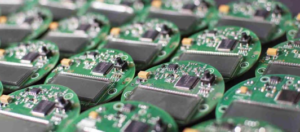
Furthermore, penalization lowers costs by increasing throughout boards. Several design parameters, particularly those pertaining to penalization techniques, are necessary for PCB penalization to be successful. In this collection of penalization rules, we’ll go into further detail about different PCB panel technologies and their particular requirements.
Optimizing for Fabrication: Considerations for Penalization Success
There are several penalization techniques, each with advantages and disadvantages of its own. Which penalization technique is most appropriate for a given application can frequently depend a lot on the layout of the board design and the PCB panel itself. Among these, the following stand out:
Design:
The board’s design has the biggest influence on whether penalization technique is best. Certain methods may be far less appropriate than others depending on the clearance between components and the board edge and whether or not there are any edge-hanging or right-angle components.

Components:
The kinds of components utilized on the board are equally crucial as where they are positioned. The best breakout and penalization technique may depend on some particularly delicate parts and connections.

Materials:
The best penalization technique may be limited by the materials used in a PCB since certain materials are more likely to split during the breakout process. The thickness of the board also matters because thin boards are more prone to break during assembly, while larger boards can cause more issues during the breakout process.
These elements restrict the options that each application can choose from.
Currently, only few penalization techniques are widely used out of the three available. They are as follows:
1. V-Score Panelization:
Individual PCBs are separated using V-shaped grooves in this popular penalization technique. Using an angled blade, these grooves take out about a third of the board’s thickness from the top and bottom. Since hand-breaking can strain the PCB and nearby components and the remaining third of the board is surprisingly strong between the grooves, a machine is typically utilized to complete the breakout operation.


2. Panelization via Tab Routing:
PCB arrays that are not feasible to utilize a V-groove technique will instead employ a tab routing technique. PCBs are pre-cut from the array using this technique, and perforated tabs hold the PCBs in position on the board. These perforation designs frequently have three to five holes. Because this technique may accommodate designs with components that hang over the edge, it is frequently advantageous. As an alternative to using tools, it can also be broken by hand.


For the majority of applications, V-Score and Tab Routing are the recommended penalization techniques. For PCB designers, knowing which of the two approaches is appropriate for their application is crucial. Designing their array for maximum strength and breakout success is the next stage. When feasible, many people use the V-groove Panelization approach due to its effectiveness and decreased surface tension. For this kind of array, depaneling equipment is likewise reasonably priced and economical. Better still, they need little upkeep and are portable.
Even though the technique typically produces board edges with more roughness, applications that use V-groove panelization rarely worry about this. V-groove penalization is better for a number of applications, but it has limitations when it comes to PCB panel design. For instance, designs where elements are positioned too near to or dangle over edges are not the best candidates for V-groove Panelization. Additionally, they present a number of production issues that need to be considered when designing, like:
3. Clearance:
A minimum of 0.05 inches of space must be kept between components and any V-grooves to prevent damage to components during the cutting process. In order to prevent the cutter from interfering with taller components, it might be necessary to move them farther away. For instance, multilayer ceramic chip capacitors surface-mounted must be spaced from the score line by at least 1/8 inch. Larger connection area components should also be positioned further away from the V-groove because solder junctions can break under the strain of depanelization if they are positioned too close to the groove.
4. Jump-Scoring:
When a PCB array is run through a wave-solder machine, V-grooves can weaken its structural integrity and cause the leading and trailing edges to droop.
Designers can add jump scoring to the array’s leading and trailing edges to fortify it and avoid these problems. One approach to achieve this is to run the V-groove about halfway through the leading and trailing array edges and add an ½ inch breakaway edge on each. Simply tell those who operate the depaneling machines to take off these breakaway edges before separating the boards. A V-scored panel should have a few issues during the manufacturing and assembly process if these design factors are considered.

DESIGN CONSIDERATIONS FOR TAB ROUTING PANELIZATION
Panelization with tab routing is typically chosen in applications where components are positioned very near to or above edges. It’s also better for PCBs that are shaped like circles or other non-rectangular geometries. To guarantee the strength and operation of these arrays, particularly during the breakout process, a number of design decisions must be made because the tabs serve as the arrays’ breaking points. Among these things to think about are:
1. Clearance:
Keep parts and traces at least 1/8 inch away from the tabs due to the stress at the breakaway points and the possibility of splintering. To ensure the least amount of interference, surface-mounted multilayer ceramic chip capacitors need to be placed further away from the tabs—at least ¼ inch.
2. Knock-Outs:
To avoid problems during the wave-solder process, a placeholder, or knockout, may be necessary if your PCB design contains holes larger than 0.6 inches. Since PCB panels are more likely to sag in the middle of an array, knockouts are especially crucial there. Larger, more irregularly shaped knockouts could require numerous three-hole perforated tabs, whereas smaller rectangular knockouts can have a wide, five-hole perforated tab on a single edge.
3. Tab Positioning:
To keep your PCB array design intact, tab positioning is crucial. For five-hole perforated tabs, tabs must be spaced every two to three inches around the edge of the board; for three-hole perforated tabs, tabs must be spaced every 1.5 inches. To prevent curvature at the board edge, tabs should be positioned as close to the edge as feasible; nevertheless, they shouldn’t be positioned beneath protruding parts. In addition, the designer needs to make sure the tabs are large enough to hold the boards in place without getting in the way of the breakout procedure.
>Place Perforations: Never run tab perforations in the middle of a tab if you want to prevent protrusions from the side of your board. Instead, run them near the edge of the PCB, or on each side if the tab is positioned between two PCBs.
4. Array Layout:
To ensure uniform break lines across the array, position all tabs that will break at the same time in a straight line (collinear). This improves panel stability during depanelization and reduces the risk of uneven board separation.
Typical benefits of PCB panelization consist of:
1. Production in bulk:
Panelization is a time and cost-effective solution if you have a large number of boards to produce. product security: The PCB is shielded from vibration and stress during assembly by panelization.
2. Swiftness and effectiveness:
Processing several boards simultaneously as part of a huge array is quicker and more effective for tasks like paste printing, component assembly, soldering, and even testing. Inconsistent break-lines can cause tabs to break in some cases and drag tabs perpendicular to the board surface in others, tearing the lamination.
If you keep these things in mind, you should have a few problems with your design when it comes to manufacturing and breaking out. Panel sizes that are standard. Manufacturing boards with the fabricator’s standard processing panel is frequently more economical. Although every manufacturer has different preferences when it comes to panel sizes, 18 x 24-inch panels typically have an ½ inch perimeter of clearance for handling double-sided boards and an inch for multilayer boards. Before writing a panel for your fabricator’s assembly procedure, you should consult with them.
Common Pitfalls and How to Avoid Them:
A PCB panel’s successful and cost-effective design depends on adhering to a few crucial rules of thumb:
1. PCB Panel size
Pick-and-place, solder past printers, quality inspection machines, and other machines in the printed circuit board production chain often specify the range of panel sizes that can vary (AOI). Because of the conveyor width, panels smaller than 2 inches, or around 50 mm, cannot be processed. Either more PCBs need to be placed on the panel or open areas around the edges need to be provided in order to prevent this issue. On the other hand, the machines also establish the panels’ maximum dimensions. The maximum dimensions for the majority of models line up with common panel sizes, like 9” x 12”, 12″ x 18″, 18” x 24”
2. Type of PCB panel
Flexible PCBs commonly have irregular or non-linear shapes. Likewise, many rigid PCBs also use these shapes to fit within installation space constraints. However, PCB panels require two straight, parallel edges for conveyor transport and easier handling. As a result, designers often add an unused handling edge around irregular board shapes. In addition, saws and milling machines have limited geometric flexibility. Therefore, the panel design also influences the choice of cutting method.
3. Distance of PCBs and spacing of cutting edges for components
Depending on the separation technique, the minimum spacing between individual PCBs can vary significantly. For example, milling requires cutting channels that are only a few millimeters wide. In contrast, laser depaneling reduces the spacing to just a few hundred µm. As a result, manufacturers can fit more PCBs onto a single panel, especially for small board designs.
When separating circuit boards, consider the spacing between individual PCBs and the cutting edge. Also, leave enough clearance around mounted components. Component height plays a key role because taller components require greater spacing. In addition, the required clearance depends on the cutting tool and depaneling method. Laser depaneling saves more panel space because its beam is much thinner than a milling head or saw blade. As a result, manufacturers can place even delicate components about 100 µm from the cutting edge without causing heat or mechanical stress.
4. Full cut of PCBs
Another way to separate circuit boards is to cut them without using tabs or V-grooves. This method is known as a full cut. Laser depaneling offers several advantages because the cutting channel and tool width are much smaller. For example, a milling machine requires a cutting channel between 2,000 and 3,000 µm wide. In contrast, a laser beam requires a channel of only about 200 µm.
This gap allows for a significant increase in the number of PCBs per panel, particularly for smaller PCBs and larger panels.
Read More: Differences between Counterbore and Countersink
Conclusion
Designing an efficient PCB panel requires careful planning and attention to several important design variables. These significantly affect the PCB production’s cost, quality, and profitability. Specifically, selecting the right separation method is crucial to the design and optimal panel utilization. In this case, mechanical processes are linked to notable constraints.
FAQs
Q. Why is PCB panelization important?
PCB panelization increases manufacturing efficiency, improves pick-and-place accuracy, reduces production costs, and protects smaller PCBs during fabrication, assembly, and depanelization.
Q. What are the benefits of doing Panelize PCB during design layout?
The benefit of the printed circuit board panelization process is a decrease in defects as automated assembly machines tend to encounter fewer problems during the assembly process. In addition, panelization also reduces costs by improving throughput.
Q. Basic points need to be ensured while proposing a PCB Panel.
PCB designers should consider the following points while panelization :
Leave additional space around the PCB panel outline for overhanging components, such as connectors, that extend beyond the board edge. You should first discuss all of your alternatives with your manufacturer as this may have an impact on the panel’s design.
Tooling Holes and Fiducial Marks: These are elements that your manufacturer will incorporate into the panel; ensure that your placement does not result in any issues.
Component Weight: If you place many components close together, the PCB panel may bend and require additional support. You can first inquire about any helpful PCB layout alternatives by speaking with your manufacturer.
PCB Width: A PCB panel may potentially bend as a result of thin circuit boards. When the panel bends while passing through the wave, this may cause issues like solder to spill over the top of some of the boards. Your manufacturer might have to use a pallet or brace the board as a result, which could affect where you arrange your components.
Q. What is depanelization in PCB manufacturing?
Depanelization is the process of separating individual PCBs from the manufactured panel after assembly. Manufacturers commonly use V-cut machines, routers, laser depaneling, or hand tools depending on the panelization method.



