Objective
This blog explains the most common PCB Design Mistakes and shows how to avoid them before a board goes into production. The goal is simple. Help readers spot problems early, improve PCB layout, and make designs easier for PCB manufacturers to build and test. PCB Runner is a natural fit for this topic because its own design and manufacturing guides keep coming back to the same idea: good boards start with clear layout rules, careful placement, and strong design-for-manufacturing checks.
Key Takeaways
- Many costly board failures begin with simple layout errors, not complex circuit problems.
- Trace width, clearance, grounding, and component placement are some of the biggest risk areas in PCB design.
- A board that works in software can still be hard or expensive to build if manufacturability is ignored.
- Early review with PCB manufacturers helps catch mistakes before they turn into delays, scrap, or rework.

1. Ignoring Design Rules In PCB Layout
One of the most common PCB Design Mistakes is starting the layout before setting proper design rules.
This causes trouble fast. Trace width, spacing, hole size, annular ring, solder mask opening, and board edge clearance all need limits from the start. If those rules are missing, the layout may look fine on screen but fail during fabrication. PCB Runner’s routing and clearance guides both stress the importance of setting design rules early and of following manufacturing limits throughout the layout process.
How To Avoid It
- Set design rules before routing begins
- Use the fabricator’s capability limits
- Run DRC checks often, not only at the end
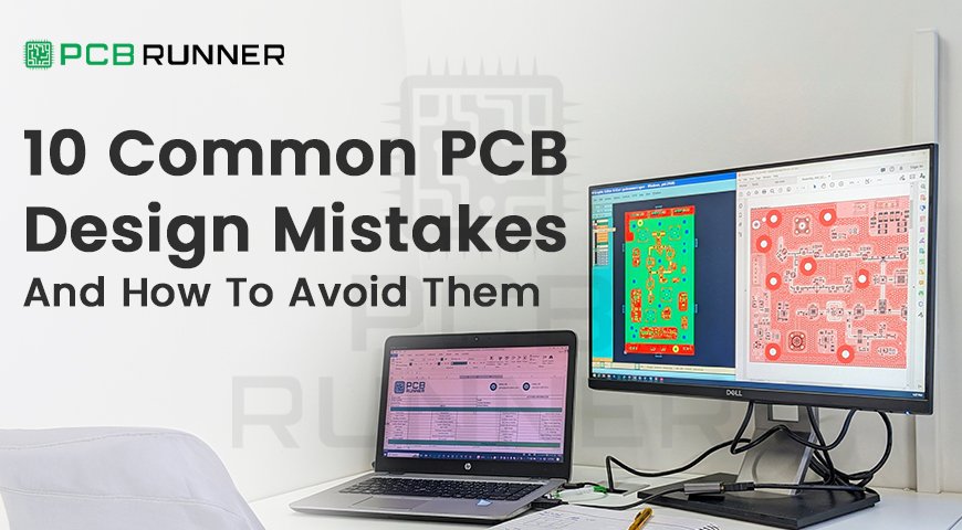
2. Using The Wrong Trace Width
A thin trace may save space, but it can also create heat, voltage drop, or weak performance if it carries more current than it should.
This is one of those PCB Design Mistakes that looks small but causes big problems later. Current-carrying traces need the right width for the load and copper thickness. PCB Runner’s routing guidance highlights proper trace sizing as a core rule for reliable boards.
How To Avoid It
- Size traces for actual current, not guesswork
- Review copper weight and temperature rise
Widen power traces early in the PCB layout
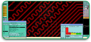
3. Poor Component Placement
Bad placement causes long routing paths, noisy signals, assembly trouble, and heat build-up.
Good boards are usually easier to understand because the placement makes sense. Related parts stay close together. Connectors sit where they need to be. Sensitive parts should be kept away from noisy or hot areas. PCB Runner’s placement guide recommends planning placement using layout tools first, then checking fit, spacing, and overall board organization before moving deeper into the design.
How To Avoid It
- Group related parts together
- Keep critical paths short
- Leave enough room for soldering, inspection, and rework
PCB Runner also appears naturally in this part of the discussion because placement problems are often found before fabrication, not after.
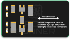
4. Weak Grounding In PCB Design
Poor grounding is one of the most damaging PCB Design Mistakes, especially in faster or noisier circuits.
A broken or poorly planned return path can increase noise, reduce signal quality, and make EMC issues harder to control. PCB Runner’s EMC and routing content both point to solid grounding and careful return-path planning as core design practices.
How To Avoid It
- Use solid ground planes where possible
- Avoid unnecessary splits in return paths
- Keep the signal and return paths closely related
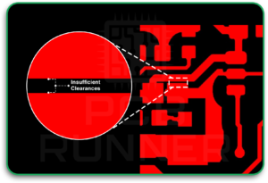
5. Inadequate Clearance Between Conductors
Too little spacing between traces, pads, or copper areas can lead to shorts, arcing, or failed manufacturing checks.
This mistake matters even more in higher-voltage designs. PCB Runner’s clearance guide says designers should set spacing rules early, account for voltage levels, and plan for the actual operating environment. Broader industry material also points to IPC-2221 as a common reference for spacing decisions.
How To Avoid It
- Set minimum spacing based on voltage and process limits
- Check copper-to-edge and pad-to-pad spacing
- Do not treat clearance as an afterthought
6. Bad Via Planning In PCB Layout
Vias seem simple, but they can create real trouble when used poorly.
Too many vias can complicate routing. Poorly placed vias can weaken current paths, hurt signal quality, or create assembly issues near pads. PCB Runner’s microvia and routing resources both stress that via structure and placement need careful planning, especially in dense boards.
How To Avoid It
- Use vias only where they solve a real routing problem
- Keep them clear of pads unless the process supports it
- Review drill size, annular ring, and plating limits with PCB manufacturers
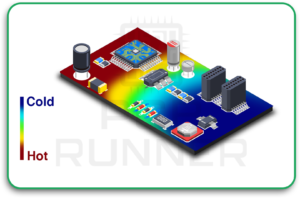
7. Ignoring Thermal Management
Heat is one of the biggest reasons boards fail over time. PCB Runner’s failure and assembly-mistake content both identify poor thermal control as a major cause of reliability problems.
A layout can be electrically correct and still run too hot. Power parts, regulators, LEDs, processors, and dense switching areas all need room to release heat.
How To Avoid It
- Keep hot parts away from heat-sensitive parts
- Use copper areas, thermal vias, or heat spreading when needed
- Review airflow and enclosure limits early
8. Forgetting Design For Manufacturability
A board should not only work. It should also be buildable.
This is where many PCB design mistakes occur. Designers may create a board that passes internal review but is difficult to fabricate or assemble at a normal cost. PCB Runner’s layout-to-lamination guide and prototyping content both stress design-for-manufacturing checks before release.
Examples include:
- Features below process limits
- Tight part spacing
- Poor fiducial planning
- Hard-to-solder footprints
- Missing assembly clearances
How To Avoid It
- Review the design with PCB circuit board manufacturers
- Match the layout to real PCB board fabrication limits
- Treat DFM as part of design, not a final box to tick
9. Choosing The Wrong PCB Material
Not every board should use the same base material.
This is one of the quieter PCB Design Mistakes, but it matters a lot. The wrong PCB material can affect heat performance, mechanical strength, signal loss, and cost. Boards used in flexing conditions, for example, may require a different structure, such as rigid-flex PCB technology rather than a standard rigid stack. PCB Runner’s manufacturing process guidance notes that material selection is an early and important stage in board production.
How To Avoid It
- Match material to temperature, frequency, and mechanical needs
- Do not choose only by cost
- Ask early whether the application needs standard rigid, high-speed, or rigid flex PCB construction
10. Skipping Testing And Prototype Checks
Skipping test planning is one of the last but most expensive PCB Design Mistakes.
Even a good-looking layout can hide problems. PCB Runner’s manufacturing process notes testing as a core stage, and its defect and prototype-related content also stresses early testing to catch faults before volume production.
How To Avoid It
- Build and inspect prototypes before full release
- Plan test access in the layout
- Review likely failure points before sign-off
A Quick View Of The Biggest Risks
| Mistake | Main Risk | Best Fix |
| Ignoring rules | Fabrication failure | Set rules at the start |
| Wrong trace width | Heat and voltage drop | Size traces correctly |
| Poor placement | Noise and assembly trouble | Place by function |
| Weak grounding | EMC and signal issues | Use solid ground planning |
| Low clearance | Shorts or arcing | Follow spacing rules |
| Bad vias | Routing and reliability problems | Plan via use carefully |
| Poor thermal control | Overheating | Add heat planning |
| No DFM review | Delays and rework | Check manufacturability early |
| Wrong material | Poor fit for use case | Choose material by need |
| No test planning | Hidden defects | Prototype and test |
Conclusion
Most PCB Design Mistakes are avoidable. They usually come from rushing the layout, skipping rule checks, or treating manufacturing like someone else’s problem. A strong board starts with simple discipline. Set the rules early. Place parts with purpose. Route carefully. Respect heat, spacing, and grounding. Then review the design with the people who will actually build it.
That is also why PCB Runner fits naturally into this topic. Its design and process guidance keep pointing to the same truth: good PCB design depends on sound decisions made long before production begins.
“A reliable board starts with a clean layout, realistic rules, and early manufacturing review.”
FAQs
1. What Are The Most Common PCB Design Mistakes?
The most common mistakes include incorrect trace widths, poor grounding, poor component placement, insufficient clearance, ignored DFM checks, and skipped prototype testing.
2. Why Is PCB Layout So Important?
The PCB layout decides how signals move, how heat spreads, how easy the board is to build, and how reliable it will be in real use.
3. When Should I Talk To PCB Manufacturers?
It is best to involve PCB manufacturers early, especially when the board has tight spacing, unusual stackups, special materials, or dense routing.
4. Can The Wrong PCB Material Cause Failure?
Yes. Using the wrong PCB material can cause thermal, mechanical, or electrical problems if it does not meet the product’s actual needs.
5. Why Are DFM Checks Important In PCB Design?
DFM checks help confirm that the design can be fabricated and assembled without avoidable cost, delay, or yield problems.
6. Is Prototype Testing Still Necessary If The Design Passed Software Checks?
Yes. Software checks help, but prototype builds and real testing can catch physical and manufacturing issues that software alone may miss.

