Objective
Help you understand Custom PCB Assembly in a clear, step-by-step way-from your first idea to a fully assembled, tested board-so you can plan better, avoid delays, and reduce costly mistakes.
Key Takeaways (If you’re in a rush)
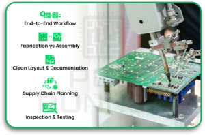
- Custom PCB Assembly is the full workflow that includes requirements, design, fabrication, parts sourcing, assembly, inspection, testing, and final pack-out.
- Printed circuit board assembly is not the same as fabrication. Fabrication makes the bare board; assembly adds parts and soldering.
- A clean pcb layout and strong documentation prevent most production headaches.
- Supply chain planning is part of electronic PCB assembly. Parts can make or break your schedule.
- Inspection and testing (AOI, X-ray, ICT, functional test) catch issues early and protect reliability.
Introduction to Custom PCB Assembly
Custom PCB Assembly is how a circuit idea becomes a real board you can plug into a product. It is more than “making a PCB.” It is also parts planning, correct placement, solid soldering, and proof that the board works.
People often get stuck because they treat this like a single step. In reality, it is a chain. If one link is weak, the final board becomes unstable, delayed, or expensive.
If you are learning this through a manufacturer like PCB runner, you will get more value by understanding the full path and what to prepare at each stage.
Why Custom Circuit Boards Matter in Modern Electronics
Custom boards matter because products have real limits:
- tight space
- heat
- power needs
- connectors that must line up
- signals that must stay clean
Did you know? Many “random” bugs in electronics are not software at all. They come from noise, weak grounding, or layout choices that looked fine on paper.
Limitations of Off-the-Shelf PCB Solutions
Off-the-shelf boards can help with demos. But they often fall short when you need:
- an exact board shape
- specific mounting holes
- clean signal paths
- a stable power design
- repeatable testing
Overview of the End-to-End Assembly Journey
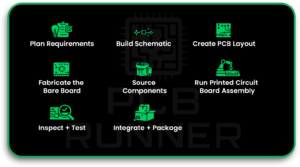
A simple view of Custom PCB Assembly looks like this:
- plan requirements
- build schematic
- Create PCB layout
- Fabricate the bare board
- source components
- run printed circuit board assembly
- inspect + test
- integrate + package
Understanding the Custom PCB Assembly Process
What Custom PCB Assembly Includes
A typical Custom PCB Assembly project includes:
- design review (DFM/DFA)
- BOM planning and alternates
- Fabrication of the pcb circuit board
- component sourcing and kitting
- SMT + through-hole placement
- soldering and cleaning steps
- inspection and test reports
- packaging and labelling
Difference Between PCB Fabrication and Printed Circuit Board Assembly
This is a common confusion:
- Fabrication: making the empty board (layers, holes, mask, silkscreen)
- Printed circuit board assembly: adding parts and soldering them
Many “one-stop” services do both, but you should still treat them as two separate stages.
Key Industries Using Custom PCB Assembly
You will see Custom PCB Assembly in:
- consumer electronics
- industrial automation
- medical devices
- automotive modules
- telecom and networking
Stage 1 – Concept Development and Requirement Planning
Defining Electrical and Functional Requirements
Start with a short, clear checklist:
- input voltage range
- current draw and peak loads
- speed or signal needs (if any)
- size limits and connector locations
- temperature range
- safety needs
Did you know? A project can “pass” in a lab but fail in the field because the temperature range was never defined clearly.
Component Selection and System Architecture
Early part choices shape everything later. Think about:
- Your main controller or logic device
- power path and protection
- connectors and mechanical fit
- sensors, radios, storage
This affects your printed circuit board (PCB) design decisions and also your sourcing risk.
Budget, Timeline, and Production Volume Planning
Volume changes the rules:
- prototypes: speed and learning matter most
- pilot builds: stability and repeatability start to matter
- mass production: yield and cost per unit matter most
In Custom PCB Assembly, planning volume early helps you pick smarter parts and a better test plan.
Stage 2 – Schematic Design and PCB Layout
Creating Circuit Schematics
A schematic is your circuit’s “truth.” Keep it clean:
- correct symbols and values
- clear net names
- obvious power and ground paths
- polarity markers for key parts
Component Placement Strategy
Placement is not “just fit it in.” Good placement helps:
- reduce noise
- improve thermal flow
- shorten critical traces
- make assembly easier
- leave room for inspection and rework
Signal Routing and Layer Stackup Planning
Routing is where many hidden problems start. You need:
- stable return paths (ground)
- correct trace widths for power
- controlled routing for sensitive signals
- a layer plan that matches the product needs
If you are doing flex and rigid pcb, you also need bend rules and keep-out zones in flex areas.
Design Rule Check and Validation
Before you send files, run checks like:
- clearance and spacing
- drill sizes
- solder mask openings
- silkscreen readability
- test points for key nets
This is one of the best “cheap fixes” in Custom PCB Assembly. Catching mistakes here avoids scrap later.
Stage 3 – PCB Fabrication and Material Selection
Choosing Substrate Materials and Copper Thickness
Material and copper thickness affect:
- strength
- heat handling
- signal behavior
- cost
Most general boards use standard materials. High-heat boards may need upgraded options.
Did you know? Copper thickness choices can also affect assembly results. Thicker copper can pull heat away during soldering, potentially requiring process tuning.
Manufacturing Processes for Multilayer and HDI Boards
More layers can improve routing and reduce noise. HDI can pack more into less space, but it also increases:
- process complexity
- inspection needs
- fabrication cost
Quality Standards and Fabrication Tolerances
Tolerances allow for variation. Tight tolerances can help:
- connector fit
- fine-pitch parts
- repeatable assembly
But tight tolerances can also raise price and lead time. This trade-off should be planned, not guessed.
Stage 4 – Component Sourcing and Supply Chain Management
Bill of Materials Preparation
A strong BOM should include:
- manufacturer part number (MPN)
- package type
- approved alternates
- notes for “do not substitute” parts
A messy BOM is one of the fastest ways to slow down electronic PCB assembly.
Authorised Component Procurement
Buying from trusted sources helps avoid:
- counterfeit parts
- wrong specs
- old stock that fails early
Even one bad reel of parts can wreck a production run.
Managing Lead Times and Part Availability
This is where schedules often break. Useful habits:
- Pick common parts early
- approve alternates
- Avoid rare packages unless needed
- Freeze the BOM before big builds
Stage 5 – PCB Assembly and Soldering Processes
Surface Mount and Through-Hole Assembly Techniques
Most boards use both:
- SMT for small, dense components
- through-hole for connectors and heavy parts
That mix is normal in printed circuit board assembly.
Automated Pick-and-Place and Reflow Soldering
A typical SMT flow:
- solder paste printing
- pick-and-place
- reflow soldering
- cleaning (when needed)
This is widely used in modern electronic PCB assembly.
Inspection Methods Including AOI and X-ray
Inspection is how you catch issues before testing:
- AOI finds missing parts, wrong polarity, and poor solder
- X-ray checks hidden joints (like BGA)
Did you know? Many solder defects are not visible from the top. That is why inspection choice matters.
Stage 6 – Testing, Validation, and Quality Assurance
Functional Testing and In-Circuit Testing
Two common test types:
- ICT checks connections and basic values
- Functional test checks real behaviour under power
If you only “power it on and hope,” you will miss problems that show up later.
Reliability and Environmental Testing
Depending on the product, you may test:
- heat and cold cycles
- vibration
- humidity
- long-run stress
Compliance With Industry Standards
Some products need strict compliance. The key is to plan early so you do not redesign at the last minute.
Stage 7 – Final Product Integration and Packaging
Enclosure Assembly and Cable Integration
Once the board passes tests, it may be assembled into a product with:
- an enclosure
- wiring harnesses
- connectors and ports
This is where mechanical details matter a lot for the final PCB fit.
Firmware Programming and Calibration
Many boards need:
- firmware flashing
- serial numbers
- calibration steps for sensors or radios
Packaging, Labelling, and Documentation
Good packaging is part of quality:
- anti-static protection
- labels with revision and date
- build notes and test summary
- handling instructions
In the middle of this stage, teams often loop back to confirm build notes with partners like PCB runner, especially when they want consistent repeat builds across revisions.
From Prototype to Mass Production
Design Optimisation for Manufacturability
This is where “it works” becomes “it builds well.”
- Add test points
- improve silkscreen for polarity
- Adjust footprints for solder quality
- reduce hand-solder steps
Scaling Production Volumes Efficiently
To scale Custom PCB Assembly, you need:
- stable BOM with alternates
- clear revision control
- repeatable test fixtures
- tracking of defects and yield
Cost Control and Yield Improvement
Yield is the percentage of boards that pass. Better yield usually comes from:
- fixing root causes
- improving inspection timing
- updating pcb layout rules based on test feedback
Common Challenges in Custom PCB Assembly
Design Errors and Signal Integrity Issues
Common issues include:
- poor grounding and return paths
- noisy power rails
- weak trace widths
- missing test points
Component Shortages and Supply Delays
A “perfect” board can still be delayed by one part. This is why alternates matter.
Manufacturing Defects and Quality Risks
Typical production risks:
- solder bridges
- tombstoning on small parts
- cold joints
- wrong polarity on diodes or caps
Best Practices for Successful Custom PCB Assembly
Early Collaboration With Assembly Experts
Bring assembly feedback in before your design is locked. It saves time and reduces rework.
Clear Documentation and Revision Control
Always package your deliverables clearly:
- Gerbers or ODB++
- BOM with alternates
- pick-and-place file
- assembly drawing
- revision history
Continuous Testing and Process Improvement
Continuous testing and process improvement treat each build like a learning loop where test results lead to findings and design updates, while defect tracking drives process changes and higher yield, which is how printed circuit board assembly improves over time.
Conclusion: Turning Your Circuit Concept Into a Reliable Product
A reliable product comes from a reliable process. Custom PCB Assembly works best when you plan requirements, build a clean printed circuit board (PCB) design, source parts with care, and test with purpose.
And when you choose an assembly partner, the “best” one is the one that matches your needs for documentation flow, inspection depth, and repeatability-so each revision becomes easier, not harder. That is also why teams that know PCB runners often focus on repeatable, quick-turn workflows as much as on the board itself.
CTA (Quote): “If you want fewer delays, lock your requirements, clean up your BOM, and add test points before the first build.”
FAQs
1) What is Custom PCB Assembly in simple words?
Custom PCB Assembly means designing a board to your exact needs and soldering all components onto it to create a working unit.
2) What is the difference between fabrication and printed circuit board assembly?
Fabrication builds the empty board. Printed circuit board assembly places components and then solder them in place.
3) What is included in electronic PCB assembly services?
It usually includes SMT/THT assembly, soldering, inspection, and testing. Some providers also handle sourcing and kitting.
4) Why is PCB layout so important?
Because layout affects noise, heat, signal quality, and the ease of board assembly and testing.
5) What files do I need to start a Custom PCB Assembly order?
Most builds need fabrication files (Gerbers/ODB++), BOM, pick-and-place, assembly drawings, and revision notes.
6) What is AOI, and why is it used?
AOI is automated optical inspection. It checks for missing parts, wrong polarity, and solder issues before deeper testing.

