You are not imagining it. PCBs are more complex to build in 2026 than they were a few years ago. Devices keep shrinking, but the boards inside them carry more signals, more power, and more heat. That pushes every step of PCB manufacturing assembly to be tighter and more controlled.
If you design boards, buy boards, or just want to understand what your vendor is doing, this blog is for you. This blog will walk you through what a modern PCB manufacturer actually does, how the PCB assembly process works in 2026, and where quality is won or lost.
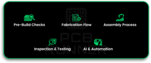
Objective
Help you understand the full PCB manufacturing assembly flow in 2026, from design checks to fabrication, PCB assembly, inspection, and testing, using simple and technically correct language.
Key Takeaways
By the end, you will know:
- What a PCB manufacturer checks before building anything
- The real step-by-step fabrication flow, and why each step matters
- The complete PCB assembly process, including SMT and mixed builds
- Which inspection and tests catch the most common failures
- How AI and automation are used in a practical
Did You Know? (Quick Facts)
- Many modern boards use HDI features like microvias and fine traces because it is the only way to route high pin-count chips in small spaces.
- BGA packages hide their solder joints beneath the PCB, so X-ray inspection is often needed during PCB assembly.
- A PCB can “pass” visual inspection but still fail later if the via plating is weak or cracked. That is why testing and process control matter.
What is PCB Manufacturing?
PCB manufacturing is the process of building the physical board that carries electrical signals inside electronic products. It involves creating copper pathways, drilling holes, plating connections, and preparing the surface so components can be soldered during assembly.
It is important to separate two ideas:
- PCB fabrication builds the bare board.
- PCB assembly places and solders components onto that board.
In 2026, PCB manufacturing is no longer just about making copper traces. It is about controlling precision. Trace width tolerances are tighter. Layer alignment must be exact. Via reliability must hold under heat and vibration.
The margin for error has become smaller because boards are denser and parts are smaller.
2) Overview of Modern PCB Manufacturing Assembly in 2026
PCB manufacturing assembly has two major parts:
- Fabrication: making the bare PCB (copper layers, holes, plating, finish)
- PCB assembly: placing components and soldering them to the PCB
The core steps are not new. What changed by 2026 was how tightly factories measured and controlled those steps. The reason is simple: the margin for error is smaller.
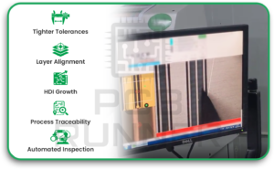
Key 2026 trends you will see from any serious PCB manufacturer:
- tighter tolerances for trace width and spacing
- better layer-to-layer alignment
- more HDI builds (microvias, blind vias)
- more process data logging for traceability
- more automated inspection to catch defects early
3) PCB Design Preparation Before Manufacturing
3.1 DFM in 2026 (Design for Manufacturability)
DFM is where many problems are prevented. A good PCB manufacturer checks your design to confirm it can be built with the selected stackup, copper weight, drill sizes, and feature limits.
A practical DFM review focuses on things that cause real failures:
- Trace width and spacing vs the fab’s capability
- Annular ring (pad around a drilled hole) so vias do not “break out”
- Drill-to-copper clearance to avoid shorts
- Solder mask slivers and dam width to prevent solder bridging in PCB assembly
- Plane clearances and thermal relief settings for solderability
- Component-to-component spacing so pick-and-place and rework are possible
What this really means is: if you fix DFM issues early, you avoid scrap and schedule slip later.
3.2 Design File Requirements
In 2026, most shops still accept classic Gerber, but many prefer formats that reduce interpretation mistakes:
- Gerber X2 (adds attributes so layers and features are clearer)
- ODB++ (packages fabrication and assembly data in one structure)
A complete release for PCB manufacturing assembly often includes:
- copper layers, solder mask, silkscreen, paste layers
- drill files (PTH and NPTH)
- board outline and cutouts
- stackup notes (materials, thickness, copper weight)
- BOM and pick-and-place files for PCB assembly
- assembly drawing (polarity, orientation, special notes)
3.3 Digital Twin and Virtual Prototyping
Not every project uses a full “digital twin,” but simulation is increasingly common. The valuable parts are usually:
- impedance checks on high-speed nets
- thermal estimates near power parts
- assembly risk checks (fine pitch, shadowing, tight keep-outs)
This helps you reduce re-spins and makes the PCB assembly process smoother.
4) What are PCB Manufacturing Technologies?
PCB manufacturing technologies describe the structural and routing methods used to build modern boards.
In 2026, the most common technologies include:
Standard Multilayer PCBs
These boards stack multiple copper layers to route signals. They are common in industrial and consumer electronics.
HDI (High-Density Interconnect)
HDI boards use:
- Microvias
- Blind and buried vias
- Fine trace spacing
This technology allows high pin-count processors to be routed in compact spaces.
Controlled Impedance Designs
High-speed interfaces require traces to maintain specific electrical characteristics. The stackup and spacing must be tightly controlled.
Mixed Technology Boards
Many products combine SMT and through-hole components on the same PCB. The manufacturing process must support both.
5) PCB Fabrication Process Step by Step (2026 Standards)
5.1 Material Selection and Stackup Planning
The stackup is the board’s layer structure. It controls thickness, impedance, and mechanical strength. In 2026, you’ll see more controlled-impedance designs as high-speed interfaces become ubiquitous.
Types of PCB Board Materials
Material selection affects electrical performance, heat resistance, mechanical strength, and cost.
The most common PCB board materials include:
FR-4
The standard material used in most electronics. It provides good strength and moderate electrical performance.
High-Speed Laminates
Used when signal integrity matters. These materials reduce signal loss and improve impedance control.
High-Tg Materials
Designed for higher temperature stability. Common in automotive and industrial electronics.
Metal-Core PCBs
Used in high-power designs where heat dissipation is critical.
RF Materials
Used in radio-frequency applications where dielectric stability is essential.
Common choices depend on the product:
- high-speed digital boards may use lower-loss laminates
- power boards may prioritise thermal stability and thicker copper
- RF boards may need materials with stable dielectric properties
A good PCB manufacturer confirms the stackup before tooling begins, as changing it later can affect impedance and drilling parameters.
5.2 Inner Layer Imaging and Etching
Inner layers are patterned first. Many factories use laser direct imaging (LDI) for fine features because it improves alignment and reduces film-related errors.
The basic flow:
- apply photoresist
- image the pattern (often with LDI)
- develop the resistance
- etch away unwanted copper
- inspect for opens, shorts, and width control
This stage is where trace accuracy is created. If it goes wrong, nothing later can “fix” it.
5.3 Multilayer Lamination and Registration
After the inner layers are ready, they are stacked with prepreg and pressed. These bond together into a single solid panel.
Registration means layers line up. Poor registration can lead to:
- Vias landing off-pad
- reduced copper capture on pads
- reliability risk under vibration or heat cycling
In 2026, improved alignment systems and registration measurement will be used more often, especially on HDI builds.
5.4 Drilling and Via Formation
Holes connect layers and support through-hole components.
You will typically see:
- Mechanical drilling for standard through holes
- laser drilling for microvias used in HDI
Microvias are small and usually connect outer layers to a nearby inner layer. They help routing density, but they also require strong process control.
Key drilling controls include:
- hole position accuracy
- smear control and hole wall quality
- drill wear and speed/feed settings
5.5 Plating, Surface Finishing, and Final Processing
Plating adds copper to the hole walls, forming electrical connections between vias.
This is a reliability-critical step. Weak or uneven plating can cause intermittent faults that show up later in the field.
After plating, the surface is finished to support soldering in PCB assembly. Lead-free finishes are standard. The “best” finish depends on shelf-life requirements, assembly temperatures, and reliability targets.
Then, the solder mask and silkscreen are applied, and final routing cuts the board outline.
6) PCB Assembly Process in 2026
6.1 SMT Assembly With Advanced Automation
SMT is the main approach for modern electronics. The standard SMT flow is:
- solder paste printing
- solder paste inspection (often used)
- pick-and-place
- reflow soldering
- inspection (AOI, X-ray as needed)
Pick-and-place machines use vision systems to correct alignment. That is important because modern parts can be tiny, and pads can be tight.
6.2 Solder Paste Printing Improvements
Paste printing is one of the biggest causes of assembly defects when it drifts.
In 2026, more lines use:
- SPI to measure paste volume and alignment
- closed-loop adjustments to reduce repeat defects
This reduces common issues like:
- insufficient solder (weak joints)
- solder bridging (shorts)
- skewed deposits on fine-pitch pads
6.3 Reflow Soldering Evolution
Reflow forms the solder joints. The profile must match the paste alloy and the board’s thermal mass.
What matters in real life:
- The board must heat evenly
- The peak temperature must be high enough to reflow correctly
- time-above-liquidus must be within paste limits
- cooldown must avoid thermal shock for some components
Smart ovens help keep profiles stable and allow traceable logs for the PCB assembly process.
6.4 Through-Hole and Mixed Assembly
Some designs still use through-hole parts for mechanical strength, high current, or connectors.
Typical methods:
- selective soldering for specific joints
- wave soldering on suitable designs
- controlled hand soldering for exceptions
Mixed technology boards are common in industrial and automotive electronics.
7) Comparison of PCB Technologies
Choosing a PCB technology depends on density, reliability, and cost.
7.1 SMT vs Through-Hole
SMT supports miniaturisation and automated assembly.
Through-hole provides stronger mechanical joints and better high-current handling.
7.2 Standard Multilayer vs HDI
Standard multilayer boards are cost-effective for moderate complexity.
HDI boards support dense routing but require tighter process control and higher fabrication cost.
7.3 Automated Assembly vs Manual Processes
Automation improves consistency and speed.
Manual intervention is still necessary for specialised components or low-volume builds.
Each approach has tradeoffs. The right choice depends on product requirements, not trends.
8) Inspection, Testing, and Quality Assurance
8.1 AI-Driven Optical and X-Ray Inspection
AOI checks visible solder joints, placement, polarity, and missing parts.
X-ray checks hidden joints, especially BGAs and some QFN centre pads.
AI can help classify defects and reduce false calls, but it does not replace a good setup. If the inspection rules are wrong, AI will not magically fix that.
8.2 Electrical Testing and Functional Testing
Electrical test checks for opens and shorts. Two common methods:
- flying probe (flexible, suitable for prototypes and low volume)
- fixture test (fast, best for high volume)
A functional test powers the board and checks its behaviour. This depends on your product. Some teams perform basic power checks; others run comprehensive firmware-based tests.
8.3 Reliability and Stress Testing
If your product runs hot, shakes, or lives outdoors, stress testing matters. Common tests include:
- thermal cycling
- vibration testing
- humidity exposure
- burn-in for early-life failures
9) Role of AI and Automation in PCB Manufacturing Assembly
Predictive Process Control
This is where AI is actually beneficial: watching process data to catch drift early. For example:
- plating thickness trending off target
- solder paste printing drifting over time
- Higher defect rates are tied to a specific feeder or stencil area
Smart Factories and Lights-Out Manufacturing
Some facilities run parts of production with minimal people during specific shifts. It works best when the process is stable and preventive maintenance is strong.
10) Sustainability and Environmental Compliance in 2026
PCB fabrication uses chemicals. Compliance is not optional. In 2026, many shops focus on:
- tighter chemical handling and waste treatment
- reduced scrap through better control
- energy savings in ovens, compressors, and plating systems
- material options such as halogen-free laminates when required
11) Supply Chain and Manufacturing Transparency
You benefit when tracking is clear. Many manufacturers provide:
- batch IDs and process records
- build status updates
- traceability for inspection and test
This improves planning and speeds up problem-solving if a defect shows up.
12) Challenges Still Facing PCB Manufacturing in 2026
Some complex parts remain:
- Skilled labour shortages in process engineering
- ultra-fine pitch assembly risks
- higher cost of advanced equipment
- balancing fast lead times with stable yields
13) How to Choose the Right PCB Technology
The right PCB technology depends on what your product must achieve.
Start by answering these questions:
How dense is the design?
If routing is tight and components are fine-pitch, HDI may be necessary.
What are the thermal demands?
Power electronics may require thicker copper or specialised materials.
What level of reliability is required?
Automotive and industrial systems demand stronger plating control and validation testing.
What is the production volume?
High-volume builds benefit from automation and fixture testing. Prototypes may rely on flexible inspection methods.
What is the cost sensitivity?
Advanced technologies improve performance but increase fabrication and assembly complexity.
Technology selection should follow engineering requirements, not marketing claims.
14) What You Should Expect From PCB Manufacturers
Here’s what a modern PCB manufacturer should provide:
- clear DFM feedback early
- stable fabrication capability that matches your design rules
- controlled PCB assembly with inspection and test options
- honest guidance on risk areas, like microvias or fine-pitch BGAs
- clear communication on lead time and constraints
15) Future Outlook Beyond 2026
Expect more of three things:
- tighter links between design tools and factory rule checks
- more automation in handling and inspection
- continued miniaturisation, which raises the bar for process control
Conclusion
In 2026, PCB manufacturing assembly is less forgiving because boards are denser and parts are smaller. The best results come from early DFM, a controlled stackup, accurate imaging, reliable drilling and plating, and a disciplined PCB assembly process with inspection and testing.
If you want a simple way to understand real-world workflows, PCB Runner is one practical reference point because it reflects how modern teams document builds, manage quality, and support consistent output.
FAQs
1. How long does PCB manufacturing take in 2026?
A simple board may take a few days. A dense multilayer board with HDI features and full testing can take one to two weeks, sometimes more if special materials or extra screening are required.
2. Are AI-driven PCB factories more reliable?
They can be more consistent because they catch drift and classify defects faster, but reliability still depends on process control, materials, and correct setup.
3. What file formats are preferred by manufacturers?
Many accept the standard Gerber format, but Gerber X2 and ODB++ are often preferred because they reduce ambiguity and include richer build information.
4. How does sustainability affect PCB costs?
Cleaner processing and compliance can add cost in some cases, but they also reduce scrap and support regulatory requirements, thereby improving overall value.

