
PCB design has evolved significantly over time. What was successful in the past ten or fifteen years is not always the case nowadays. Signals travel at a faster rate, boards are smaller, and components are packed more closely together. As a result, signal integrity analysis for PCB design is now an increasingly important issue in the design of modern PCBs.
Many designers still use traditional techniques. These approaches are focused on connectivity and not behaviour. This strategy is no longer working. To create reliable boards today, designers need to understand the way signals behave and how they can be controlled.
At PCB Runner, engineers frequently tackle designs where performance is crucial in real-world conditions within Europe, the UK, and elsewhere. This article will explain how to overcome problems with signal integrity and create PCBs using more advanced techniques with simple logic and practical thought.
Why are traditional PCB Design Methodologies Not Effective?
Traditional PCB design workflows evolved when digital signal edge rates were slow relative to trace lengths, making transmission line effects less dominant. Traces could often be treated as lumped elements rather than transmission lines. Designers did not have to be concerned about reflections, noise, or even timing.
The circumstances have changed.
Today’s designs include:
- Speedier switching speeds
- Tighter timing margins
- Higher routing density
- Smaller layer spacing
These changes directly lead to the integrity of PCB signals at high speeds.
The traditional rules, like fixed trace widths, or even basic spacing guidelines, fail to look at how signals behave when operating when they are operating at high speeds. This is why problems typically show up late, in testing, or even after the manufacturing process has finished.
This is the reason signal integrity analysis for PCB design is now a necessity rather than a supplementary option.
What does Signal Integrity really mean for Modern PCB Design
Signal integrity is the quality of an electronic signal to reach its destination:
- The right level of voltage
- Just at the right moment
- With minimal distortion
Signals propagate as electromagnetic waves along PCB interconnects, making transmission line effects dominant. This is because of the transmission line effects in PCB design.
Even if the frequency seems low, the fast edge rates could still result in:
- Reflections
- Ringing
- Crosstalk
- Timing errors
If these issues are not adequately controlled, the system can be unable to function properly, which is usually the most challenging kind of failure to identify.
How traditional design practices can cause Signal Integrity Issues
Many issues with signal integrity are not due to defective components. They are a result of poor design practices.
1. Relating Traces to simple wires
In the traditional layout, the traces are drawn in order to join pins. The electrical properties of the traces are often overlooked.
This is the reason:
- Impedance that is not controlled
- Reflections caused by impedance discontinuities along the signal path
- Sign distortion
Inattention to the impedance control trace specifications is among the most frequently made mistakes.
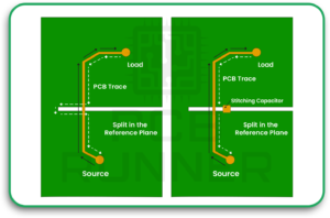
2. Insisting on the Return Path
Every signal requires an exit path. This return path is usually through the reference plane.
Problems can arise when:
- Ground planes are divided
- Signals are able to cross the plane and create gaps
- Return currents are compelled to divert
This can cause noise to increase and decrease the signal’s quality.
3. Fixing Problems Too Late
The attempt to repair signal problems after the routing process is completed is not always successful. After that, the stack-up and layout options are restricted.
It is better to incorporate signal integrity analysis for PCB design prior to the routing process beginning.
Prioritising early to avoid Signal Integrity Problems
The process of moving beyond traditional methods begins with making plans.
1. Define Electrical Constraints Early
Do not guess; you should define:
- Values of the impedance target
- Maximum skew
- Acceptable signal loss
These limits guide every design decision.
2. Topology for Plan Routing in advance
Different signals require different methods of routing.
Planning helps to avoid:
- Long stubs
- Excessive vias
- Poor choice of termination options
This helps to eliminate high-speed PCB signal integrity issues. problems before the layout process even begins.
Stack-Up Design is Beyond Traditional PCB Thinking
The Stack-up design is among the most effective methods to improve the Signal Integritys.
1. Impedance Control PCB Stackup
An impedance control stackup PCB determines how the layers are arranged, as well as the thickness of the dielectrics.
It allows the designers to create precise impedance values, instead of having to rely on intuition.
A well-planned stack-up
- Reduces reflections
- Improves timing
- Facilitates routing
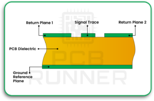
2. The Continuous Reference Planes
High-speed signals require solid reference planes.
Good practice should include:
- Continuous ground planes that are continuous under a layer of signal
- Beware of plane splits on crucial routes
- Minimising reference plane changes
These steps significantly improve the stability of signals.
3. Making the Right Materials
Standard FR-4 can be used with a variety of models. As speeds increase, loss increases.
In these cases, the use of low-loss materials can help to reduce attenuation and help preserve the signal’s shape.
PCB Trace Routing for SI beyond Old Rules
Routing is the place where the theory meets reality.
Make sure that the Trace Geometry is Consistent
For efficient PCB trace routing for SI ensure:
- Consistent trace size
- Stable spacing
- Smooth transitions
Unexpected changes in geometry trigger reflections and changes in impedance.
The Differential Pair Routing, Done Correctly
Matching length alone is not enough.
Good differential routing also demands:
- Constant pair spacing
- Symmetry between trace
- Modest layer changes
This decreases noise and increases timing precision.
Managing Vias Carefully
Vias introduce discontinuities.
To minimise their impact
- Use fewer vias
- Keep via stubs short
- Use back-drilling if necessary.
These steps will help maintain the quality of signals.
Also Read
- From Past to Future: Trends in PCB Design
- Step-by-Step Guide to Medical PCB Design for Medical Devices
Crosstalk Mitigation Techniques PCB Designers Must Make Use of
As the density of routing increases, crosstalk becomes more challenging to avoid.
Effective crosstalk-reducing techniques that PCB designers utilise include:
- Increase spacing wherever it is
- Beware of long parallel runs
- Routing adjacent to solid reference planes
- Utilising ground shielding to protect sensitive signals
Crosstalk isn’t just about spacing. Quality of the return path plays a crucial role.
Signal Integrity and Power Integrity are Linked
Signals can’t be pristine when power is shaky.
Power noise causes:
- Jitter
- Timing errors
- Power noise reduces noise margins
To help ensure the integrity of the signal:
- Place decoupling capacitors close to IC pins
- Make use of multiple capacitor values
- Maintain power planes with low impedance
A stable power system supports steady signals.
Making Use of Signal Integrity Analysis for PCB Design to Go Beyond the Limits of Guesswork
Simulation allows designers to anticipate the behaviour of hardware before it is constructed.
Pre-Layout Analysis of Signal Integrity
This analysis examines:
- Topologies of routing
- Strategies for termination
- Options for stacking up
Utilising signal integrity analysis for PCB design early will reduce the need for rework.
Check-up of Post-Layout
After routed after routing, the analysis confirms:
- Consistency of the Impedance
- Reflection levels
- Crosstalk is a risk
This will ensure that the design meets expectations for performance.
Verifying Designs by TDR Testing
Simulation is crucial, but measurement is crucial.
TDR testing helps:
- Verify impedance
- Identify discontinuities
- Confirm the accuracy of the stack-up
The combination of simulation and the testing of TDR increases confidence in the end product.
Designing for Manufacturing Without Reintroducing Problems
Variations in pcb manufacturing can impact the quality of signals.
Designers should consider:
- Trace width tolerance
- Dielectric thickness
- Copper roughness
- Etch compensation
- Resin content variation
A clear communication between the design and fabrication teams is essential to ensure the sameness between UK and European production.
Practical Experimentation of a Method that is Moving Beyond Traditional Strategies
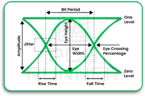
Take a look at a high-speed connection that does not pass the test of the eye diagram.
Traditional fixes can slow down the signal.
The best approach is:
- The impedance control PCB is being updated with a stackup
- Enhancing PCB trace routing to SI
- Reducing via stubs
- Implementing the correct crosstalk mitigation techniques PCB layouts are often missed
This method addresses the root of the problem.
Best Practices Checklist
- Signal integrity of the plan right from the beginning
- Limits on timing and impedance
- Utilise controlled stack-ups
- Maintain continuous return paths
- The geometry of the route trace is consistent
- Validate using simulation and measurement
Conclusion
Today, designing PCBs that are durable means expanding beyond the conventional methods.
By focusing on signal integrity analysis for PCB design, engineers can create boards that work consistently in real-world situations.
With this method, PCB Runner creates designs that meet current expectations for performance across Europe, and the UK.
Signal Integrity is no longer just a matter of. It is the foundation for an effective PCB design.
FAQs
1. What is signal integrity analysis? What does it mean for PCB design? Why is it important?
Signal integrity analysis for PCB design will predict the way the signals will behave on a PCB and assist in preventing reflections, noise, and timing mistakes prior to manufacturing.
2. What are the problems with the integrity of PCB signals at high speeds that influence performance?
High-speed PCB signal integrity issues could cause malfunctioning data, unstable operation, and even test malfunctions, even if components are functioning correctly.
3. What is the importance of impedance control PCB stackup so critical?
A stackup of impedance control PCBs guarantees predictable signal behaviour and helps reduce reflections and timing issues.
4. How can PCB trace routing for SI help reduce noise?
PCB trace routing for SI is based on a consistent geometry, proper spacing, and solid reference planes, which stabilise signals.
5. What’s the reason behind TDR testing used in signal integrity analyses to design PCBs?
TDR testing validates the impedance of the actual circuit and confirms that the board is in line with the original design.

