
When people think about PCB delays, they usually blame parts, layers, or “fab capacity.” But one of the most common hidden causes is much simpler. It is your PCB outline.
The outline is not just a shape on your screen. It is a manufacturing instruction. It tells the factory how to cut the board, how to panelize it, and how to separate it after assembly. If your outline is unclear or overly complex, the factory cannot “guess.” They have to stop and ask. That means extra back-and-forth, more checks, and more time.
At PCB Runner, we often see designers focus heavily on routing and forget that the mechanical boundary is also part of the engineering work. This article will help you avoid that mistake.
You will learn how mechanical design for PCBs and outline decisions impact price and schedule, from EDA export to fabrication and assembly. You will also get simple rules you can use on your next release.
PCB Outline Best Practices in EDA: What the PCB Outline Really Means
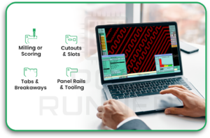
A PCB outline is the exact boundary of the board. It tells the fab shop:
- Where to route or score the board
- Where internal cutouts and slots are
- Where tabs or breakaway features may be needed
- How much room exists for panel rails and tooling
In fabrication terms, the outline is a “toolpath” instruction. It becomes a routing path or a scoring line. That is why the outline impacts both lead time and cost.
PCB Outline Practices for files and layers
To avoid delays, always provide:
- One closed outline on a clear mechanical layer
- One outline only (not multiple versions on different layers)
- A fabrication drawing that repeats the outline information in plain words
Factories see many CAD tools and many export styles. A clean outline reduces questions.
Mechanical Design for PCBs: How to Define the PCB Outline Correctly
Most outline problems start inside the EDA tool. Common mistakes are small, but they cause significant delays later.
For “single clean closed contour”
Your outline should be:
- A single closed shape
- No gaps
- No overlaps
- No duplicate lines
- No tiny “spikes” or accidental bumps
If the factory’s CAM engineer cannot tell which line is “the” outline, they must email you. That adds time.
For PCBs and tolerances
A tight tolerance can increase cost and time. Why? Because it can require:
- Slower routing
- Extra inspection
- Special fixturing
If you do not need a tight tolerance, do not demand one. Use normal tolerances unless the enclosure truly requires it.
From EDA to Fabrication: Why Outline Complexity Adds Lead Time
Simple shapes move faster through manufacturing. Complex shapes do not.
A rectangle with rounded corners is usually quick to process. A shape with many tiny curves, sharp internal corners, or narrow protrusions is slower.
Best practices for faster CAM approval
Outline complexity increases:
- CAM review time (more chances for errors)
- Routing time per panel
- Risk of breakage during depanelisation
- Scrap risk, which can raise the price
If you want a short lead time, keep the outline simple whenever possible.
Internal Cutouts, Slots, and Cavities: Small Features That Add Big Cost
Internal cutouts look harmless in CAD. But every cutout can add machining time.
PCB outline practices for slots and cutouts
These features can trigger extra work:
- Internal routing (the tool must enter, cut, and exit)
- Narrow slots that force small routing bits
- Many repeated cutouts, which increase the machine cycle time
A simple rule:
- Keep slot width reasonable.
- Avoid tiny slots unless they are necessary.
- Combine cutouts where possible.
For sharp internal corners
Sharp internal corners are harder to make. Most routing tools create rounded internal corners because the tool is round. If your design needs a sharp corner, you may need special processing or design changes.
Depanelisation Choice: Route, V-Score, or Tabs (And Why It Matters)
Even if your board shape is simple, your separation method matters. It can change both lead time and total project cost.
PCB Outline Practices for V-Score depanelisation
V-scoring is fast and often low-cost. But it has a limitation.
V-scoring works best when:
- The board edges are straight
- The panel lines run edge-to-edge
- You can accept the scoring rules
If you request a V-score on curves or odd shapes, you will get questions and delays.
PCB Outline Practices for routed tabs and mouse bites
For odd shapes, routing with tabs is common. But it adds:
- More routing time
- Tab cleanup time after depanel
- Possible stress damage if tabs are placed poorly
Tab placement matters. Tabs near connectors or fragile parts can increase assembly defects.
Panelization and Utilisation: The Biggest Hidden Cost Driver
Many people think the board’s “area” is the only cost factor. But the outline also affects how well the board fits into a panel.
A board that nests well wastes less space. A board with protrusions and odd curves wastes more space. You often pay for the wasted panel area, too.
Mechanical design for PCBs and panel rails
Factories often add rails for:
- Conveyor support in assembly
- Tooling holes
- Fiducials for pick-and-place
If your outline gives no room for rails, the factory may need to change the panel plan. That can add time and extra cost.
This is also where your plan changes if you are doing a turnkey PCB build, because panel handling affects both fabrication and assembly steps.
Copper-to-Edge, Edge Plating, and Beveling: Outline Decisions That Trigger Special Processes
Outline choices are not only about shape. They also affect edge processing.
PCB outline practices for copper-to-edge clearance
If copper is too close to the board edge:
- Routing can expose copper
- You may get shorts or delamination risk
- The factory may request a redesign or ask for edge plating
This back-and-forth can slow your release.
Edge features
Some edge features add cost and lead time:
- Edge plating
- Castellations
- Bevelled edges (for card-edge connectors)
These steps may require special tooling and extra inspection. They often add days, not hours.
PCB Assembly in Europe and the Outline
Even if fabrication is fine, assembly can still be affected by outline choices.
For PCB assembly in Europe, factories often use standardised conveyors, support pins, and fixtures. Odd outlines can cause:
- Poor support during stencil printing
- Board movement during placement
- Warpage risk during reflow
- Increased need for custom pallets
PCB outline practices for assembly-friendly shapes
To keep the assembly smooth:
- Avoid fragile “ears” or narrow extensions
- Keep a stable overall board shape
- Place fragile parts away from breakaway edges
- Use rails when needed for support
If the board must be a complex shape, call it out early. That helps the assembly team plan fixtures.
Lead Time Breakdown: Where the Outline Adds Days
Here is where outlines usually cause delays:
- CAM questions: unclear outline layer, multiple outlines, open shapes
- Tooling setup: special routing, internal cutouts, and bevel needs
- Routing queue: complex routing takes longer per panel
- Depanel planning: V-score vs routing decision confusion
- Yield issues: fragile shapes break during handling
A clean outline reduces all of these.
Cost Breakdown: How the PCB Outline Changes Your Quote
Outline-driven costs usually come from these sources:
- Routing time: more complexity means more machine time
- Panel waste: poor nesting means you buy more panel area
- Special steps: beveling, edge plating, castellations
- Extra inspection: tight tolerances and complex cutouts
- Assembly handling: pallets, rails, and slower line speed
For a turnkey PCB order, these costs can stack because you are paying for fabrication and assembly impacts together.
Also Read
- PCB Technology: Transforming Innovation in Electronic Devices
- Future-Forward: Trends Driving PCB Fabrication Today
Best Practices That Reduce Cost and Lead Time
Here are practical rules you can apply right now:
Keep the outline simple when possible.
- Prefer rectangles or rounded rectangles
- Avoid unnecessary curves and tiny details
Use generous internal radii.
- Routing tools like smooth turns
- Sharp corners increase complexity
Make cutouts intentional, not accidental
- Limit the number of internal cutouts
- Keep slot widths realistic
- Avoid tiny isolated “islands” of board material
Decide on depanelisation early.
- If you want a V-score, design for straight edges
- If you want routed tabs, plan tab placement away from fragile areas
Make assembly support easy
- Leave room for rails if needed
- Keep heavy parts away from breakaway edges
- Think about handling, not only the electrical layout
A Simple Pre-Quote Checklist
Before you send files out, run this checklist:
- One closed, clean outline on the correct layer
- Outline shown in the fabrication drawing
- Internal cutouts are clearly defined
- Depanel method stated (V-score or routed tabs)
- Any special edge processing listed
- Copper-to-edge clearance checked
- Rails and tooling needs considered
Doing this can save days of email.
FAQs
1: What are the best PCB outline practices that reduce lead time the most?
The fastest PCB outlines are using one clean, closed outline, avoiding tiny cutouts, and choosing a simple depanel method, because these practices reduce CAM questions and routing time.
2: How does mechanical design for PCBs affect lead time and cost?
Good mechanical design for PCBs keeps outlines simple, sets realistic tolerances, and avoids fragile shapes, and this reduces routing complexity and scrap risk.
3: For PCB assembly in Europe, do odd board shapes increase assembly time?
Yes, for PCB assembly, very irregular shapes may need rails or custom support, and PCB assembly lines may slow down when boards do not sit flat or stable during printing and reflow.
4: Does a turnkey PCB order cost more if the PCB outline is complex?
Often, yes, because a turnkey PCB build includes both fabrication and assembly impacts, and a complex outline can raise turnkey PCB cost through extra routing time, panel waste, and fixture needs.
5: What PCB outline best practices help when I need routed tabs and mouse bites?
For routed tabs, PCB outline best practices include placing tabs away from connectors and fragile parts and keeping breakaway edges clear, because these practices reduce damage and rework.
Conclusion
Your PCB outline is not just a border. It is a key part of the manufacturing plan. A clear, simple outline reduces questions, speeds CAM approval, improves panelisation, and prevents assembly handling problems. Complex outlines can still work, but they should be intentional and designed with routing, depanelisation, and support needs in mind.
If you treat the outline as part of the engineering work from day one, you will usually get faster quotes, fewer surprises, and a smoother path from EDA to finished boards. And for teams learning these handoff details, PCB Runner is a valuable place to connect design choices with real production outcomes.

