Schematic & BOM Formation

Schematic & BOM Formation

Mastering PCB Design: From Schematic to BOM and Production – A Comprehensive Guide by PCB Runner

A consistent visual depiction of a circuit can be found in a schematic diagram of a circuit board. One of the most important aspects of PCB design is the schematic diagram. A sample circuit board schematic can show how different electronic components are connected. This could be the first action in a device’s strategy. Earlier, circuit charts were drawn by designers on paper. They have started using PCB plan instruments, which simplify the plan preparation process. A well-drawn PCB schematic diagram can significantly reduce the need for later PCB rework.

Creating a Clear and Accurate Schematic 

Follow conventional schematic guidelines to create an efficient schematic design.

Page size selection:

The majority of design programs include many page sizes. Depending on how much their circuit plan is estimated, the designer might choose it. 

Page naming accord:

The schematic’s logical blocks are divided into pages. Pages are arranged alphabetically by us. Most designers edit the history instead of block charts to save time. When other designers attempt to comprehend the schematic diagrams, they are accommodating. The majority of the organizations participating followed each of these guidelines and customs. 

Grid Settings

The tool needs some reference, but the designers are not immediately required to provide this. Designers can more accurately reference and connect parts when they use a grid. Throughout the examination, circuit components need to be continuously connected to the grid and open to network probing.
Page title bar: The page title bar completes all the required information and is situated in the schematic page’s footer. (Page size, modification date, record number, name and purpose of the circuit, and disclaimer from the manufacturer).
Remarks: The circuit’s relevant annotations must be written by the designers. Messages can be written on pages of schematic drawings or stand-alone papers. Annotations for intricate patterns are frequently given on different pages. Jumper states and PCB layout limitations and guidelines are a few of the remarks.

Revision history:

 Revision history documents alterations made to the layout. The date, a summary of the modifications, the names of the authors and reviewers, and the review comments are all included in the document. Usually, the main or last page of the schematic layout contains the revision history.  Directory of schematic documents: This directory contains a list of the subjects covered in the schematic documentation. This website makes it simple for designers to locate particular modules inside a complex design. If the operation is modest and has a straightforward design, you can omit it.  

Block diagram: 

Block diagrams significantly aid reviewers in understanding the design for a review by speaking to various modules within the plan and flag flow.

Network label agreement: 

The schematic is meant to simplify the circuit for designers to understand. The common symbols of an integrated circuit (IC) in PCB design can be reduced when creating a schematic by minimizing the number of unnecessary network connections. Instead of dragging a bunch of networks across the screen, the designer refers to the well-organized title of a specific stick that is connected to a trap on another device. The names of these pins will be the same. The readability of the schematic diagram is increased by assuming that a pin with the same name is connected. When a network is directly connected to another IC on the same page, network naming is not necessary. But you must give it a name if you wish to link the network to an IC on a different page.

Design rules checking: 

A clever CAD function called Design Rule Checking (DRC) verifies the logical and physical integrity of a design. The online check can be completed at plan time and is based on all empowered plan rules.
Verification of net tables: 

Create the netlist as soon as the schematic design is finished and the layout is imported. There are two possible extensions for net table files:mnl and.txt. While the.txt file shows every electrical connection between components, the.mnl files are machine-readable. To prevent design flaws, it is advised that the network be manually verified.

Bill of Materials

BOM generation is currently a crucial capability offered by the CAD tool. If the designer provides all inputs in the tool when building or importing parts from the library, you can generate a complete and sufficient BOM. The manufacturing part number (MPN), package, supplier name, and supplier part number are among the details that can be found on the bill of materials. It is advised to provide all pertinent data while creating symbols.

Beginning with circuit boards, the Bill of Materials, or BOM, is an essential component of any electronic device’s design and manufacturing process. The project might require adjustments in the absence of a comprehensive BOM, which could delay production. As such, one of the most important factors in PCB production is the BOM.

Most of the time, when a customer submits an order, manufacturers request that they upload their BOM list. Nonetheless, it is essential to understand the data that a BOM should contain while designing one. The required information should also be included in the bill of materials. BOMs provide several advantages to consumers and electronic manufacturers alike. Thus, before creating one, it’s critical to comprehend what a bill of materials comprises.

A Bill of Materials: What Is It?  

A list of materials, parts, and assemblies needed for product manufacturing is called the bill of materials. Production depends on the data in the bill of materials. Consequently, to produce a product, producers must rely on these bits of information. The BOM needs to be extremely precise and well-detailed. The BOM determines a production’s level of success. 

BOMs are essential for producers as well as customers. When a customer orders circuit boards, for example, it is helpful for them to express their needs. To manufacture the circuit board or electronics according to the customer’s requirements, the PCB assembler uses this information. The BIOM can also be used as an ingredient list when producing a product. Creating a BOM is the first step in the production process for all manufacturers. This is so because the product’s basic specifications are provided by the BOM. BOM is utilized by several production sectors in addition to the electronics industry. As the phases progress, the BOM also improves production.

Electronic components list with highlighted item for a momentary push button switch.

How to make clear and well-organized schematics Space

You must choose how to use the blank space that appears when you first open a new schematic. It relies on several variables, including the project’s size and complexity, target audience, any standards you must adhere to, and the project’s expected life cycle. Additionally, it depends on whether or not you need to print the schematic.
Whether you need more than one sheet or if one will do is the most crucial decision to make. Starting with a single A4 page and switching to an A3 sheet as the project progresses is one method for smaller projects.

The Best Component Arrangement for Understanding and Clarity  

Logic and Intuition-Based Component Arrangement

 To Reduce Signal Crossings and Improve Flow  

 Making Explicit and Brief Connections Selecting Line Styles and Thickness that are Correct Steer clear of overlapping and unclear connections Assigning Names, Nodes, and Component Labels  

Component Labeling: 

Every element in the schematic diagram needs to have a label that corresponds to its reference designator. Alphanumeric identifiers known as reference designators are used to identify each component separately. It is important to label the components suitably once the schematic design has been constructed and they are each represented by a symbol. The circuit design is made clearer and easier to understand by labeling parts, nodes, and signal names. 

Labeling Nodes:

 In a circuit, nodes are the locations of connection between various components. Voltage nodes (e.g., Vcc for positive power supply, GND for ground), signal nodes (e.g., IN for input, OUT for output), and particular node labels pertinent to the circuit design are examples of common node labels. Troubleshooting and circuit analysis are made easier by labeling nodes. 

Labeling Signal labels:

 It’s important to give the right labels to the signals in the schematic diagram in addition to labeling the components and nodes.

The purpose or function of a specific electrical or electronic signal inside the circuit is described by its signal name. “CLK” for clock signals, “DATA” for data signals, “RESET” for reset signals, and “ENABLE” for enable signals are a few instances of signal names.  Examining and confirming the schematic diagram. Performing Extensive Quality Inspections to Verify Completeness and Accuracy  Getting Input from Experts or Peers to Verify.

Guidelines for Component Selection  

Comprehending Component requirements: 

To start, make sure you fully comprehend the mechanical and electrical requirements of the components you require. Temperature tolerances, package sizes, voltage and current ratings, and package dimensions are important factors.  

Component Availability: 

Take lead times and component availability into account. To avoid project delays, make sure that the selected components are easily obtained from vendors.

Cost vs Performance: 

Aim for a balance between the cost and performance of the components. Although cost control is crucial, sacrificing component quality might result in reliability problems.  

Environmental Considerations: 

Choose components that can survive harsh circumstances, such as high humidity or extreme temperatures, if your PCB will be operating in these kinds of settings. 

Verify that the components are compatible with the footprint libraries and PCB design tools of your choice.

Longevity: 

Consider a component’s long-term availability, particularly if your project calls for lengthy production cycles.

Validation of Design and Simulation  

Design Validation: 

Verify the functionality, signal integrity, and thermal performance of the design using simulations and studies.  Iterative Refinement: Fix any problems found during validation and make the required changes to the design.

Design Records  

Design File Creation: Produce thorough design files that include manufacturing comments, assembly drawings, bill of materials (BOM), and Gerber files. The files known as manufacturing data, which include copper layers, solder masks, and other components, are what will be used to construct the etched base laminate on your PCB. The exported data in these files was produced from your CAD designs. It’s critical to maintain track of the versions of your files and ensure that the proper version of your CAD design is linked to each file by a clear naming convention.

It is possible, if challenging, to reverse engineer your manufacturing data from an existing PCB. To ensure that you’ll be able to have the source documentation to quickly build your files for manufacturing, it’s critical to keep your design files, record revisions, and back up your data. Cooperation: To ensure efficient production, distribute design documentation among team members, fabricators, and assemblers.

The Importance of Software for PCB Design  

Your PCB design is created on a digital canvas using PCB design software. It gives designers the ability to precisely route traces, layout components, and build schematics.  Your ability to collaborate, design efficiency, and the quality of the finished project are all impacted by the software you choose.

Advice on Which PCB Design Software to Choose  

Selecting the appropriate PCB design software should be in line with your level of experience and the demands of your particular project. Here are some pointers to think about:  

Evaluate the level of difficulty involved in your project. Simple designs can be satisfied with inexpensive, user-friendly software. High-end software with sophisticated functionality could be needed for complex undertakings.

Learning Curve: Take your experience with PCB design software into account. While some programs offer advanced features but may have a longer learning curve for beginners, others may be more user-friendly.

Compatibility: Verify that the program you select can import and export the required file types and is compatible with your operating system.  

Collaboration: Choose software that allows for both version control and real-time collaboration if you’re working in a group.  

Cost: Consider the licensing, upkeep, and extra features while evaluating the software’s cost structure. Remember your financial limitations.  

Support and communities: Look into the resources, forums, and user communities that are available to help you when you run into problems.  

Future Scalability: Consider if the program can grow with the project in the future and adapt to changing design specifications.

Trial Period: A lot of software vendors provide free trials. Use these to see if the software is appropriate for the task at hand.  A crucial first step in making sure your PCB design project is successful is selecting the appropriate PCB design software. You may make an informed decision that will enable you to implement your PCB design ideas successfully and efficiently by considering the particular requirements of your project, your degree of experience, and your financial constraints.

Common Software Tools for PCB Design  

A wide variety of PCB design software solutions are available to meet different design needs and user preferences. Among the software tools that are most frequently used are:  Altium Designer: Preferred by expert PCB designers, Altium Designer is renowned for its intuitive UI and robust features. It has tools for capturing schematics, arranging components, and collaborating in real-time. 

Eagle: Autodesk’s Eagle is well-known for being both inexpensive and easily accessible. With a large library of components, it’s appropriate for novices as well as enthusiasts.

KiCad: This open-source program is well-liked for its wealth of capabilities, which make it an affordable alternative for novices and experts alike. 

Cadence Allegro: Because of its excellent routing and seamless connection with other design tools, this dependable program is used.  

OrCAD: OrCAD provides a full range of tools for PCB design, such as simulation, PCB layout, and schematic capture.
Siemens’ PADS offers a variety of design functionalities and is appropriate for small and medium-sized enterprises. 

Best Practices for Schematic Capture for Easily Read Schematics  

Schematics must be simple to read and comprehend by users in addition to having intelligent components and connectivity features. Layout engineers, component engineers, manufacturing staff, test technicians, and field repair specialists will all use them. They must so explain in detail what their circuitry is doing. When designing a schematic that will be helpful to everyone, keep the following points in mind:

Parts Arrangement: Try to arrange the parts in a clean, well-organized manner. Resistors and other parts should be arranged in rows with enough room between them for text and nets. People farther down the line may find it more difficult to quickly discover a certain element if components are placed on a schematic haphazardly.

Signal pathways: The order of components should be based on their respective signal pathways. The path must begin from the driver pin, follow a logical flow through the circuit, and terminate at the end. This not only improves the design of your schematic and frees up space for more circuitry, but it also makes the circuit easier to grasp for the layout team to work with.  

Give Yourself Room to Grow: Your schematic may expand when new features and improvements are introduced, even though it may shrink in size initially. It is wise to allow space for the addition of more circuitry as needed because of this. If nothing else, you’ll probably adjust and revise as you create, and having more space makes it much simpler to move parts and nets around.

Net Connectivity: Just like with component placement, everyone’s work will be much easier if the nets flow in a tidy and ordered manner. Buses ought to be clustered together wherever feasible. Seeing how the busses are arranged and the flow of the signal routes will be especially helpful to the layout team when they are floor-planning the PCB layout.

Don’t Forget the Details: Your schematic isn’t finished when all the parts are arranged and routed together. To make the reference designators readable, they must be shifted and rotated. This also applies to net and bus names, which for readability purposes should be aligned in the same direction as their wires. Dates, other firm information, and board names and numbers must be entered into title blocks. Finally, remember to include any special notes or design information that will aid in the layout, production, and repair of those who utilize the schematic.

Common mistakes during BOM creation

Reason for error: Failure to include all required parts in a Bill of Materials (BOM) is a frequent error. This error may be the result of carelessness or insufficient detail in the BOM creation procedure.  Examples: Let’s say a company is making complicated electronic equipment that needs a variety of screws, but the BOM just lists a small number of them. In that scenario, as they wait for the missing screws to arrive, the manufacturer might have to stop manufacturing or postpone shipping. As an alternative, the device might not function properly during testing or usage because the maker used the wrong kind of screws.

How to avoid: Manufacturers should create their BOMs methodically to prevent making this error. This process should begin with a thorough analysis of the product design to determine all the components and materials that are required. To detect any omissions or mistakes, it is crucial to make sure that the BOM is examined by some people, such as engineers, buying managers, and production supervisors. Manufacturers should also routinely update their BOMs to account for modifications to component availability or product design. Ultimately, to guarantee that any modifications to the BOM are accurately recorded and shared with all parties involved, manufacturers must put in place a thorough change management procedure.

Not indicating the precise number of pieces

Neglecting to include the correct number of pieces in the Bill of Materials (BOM) is another typical error. Errors in the conversion between units of measure or inaccurate estimates about the quantity of parts required can result in this issue. As an illustration, let’s say a company has to make 100 units of a product but orders 10 units of a crucial component by mistake rather than 100. Then, there could be a delay or stop to the production process, which would mean lower profits and higher expenses. Alternatively, let’s say a manufacturer orders the incorrect quantity of a component, causing delays in manufacturing or material waste, because they specified the incorrect unit of measurement.

How to stay away from: Manufacturers should be very careful when indicating the right number of pieces in their BOMs to prevent making this error. To make sure the values are correct, they should verify all computations and conversions between units of measurement again, as well as get feedback from a variety of stakeholders. Manufacturers should also put in place a strong quality control procedure to identify any mistakes before they affect production. Lastly, to account for any modifications to manufacturing specifications or product design, manufacturers should constantly review and update their BOMs.

Failing to update the BOM

Justification for the error: Failure to update a Bill of Materials (BOM) regularly is another typical error made when creating one. Manufacturers may make this error by neglecting to take into consideration modifications to the production procedures, material availability, or product design.  As an illustration, let’s say a manufacturer releases a new version of a product, but the BOM that was used to make it isn’t updated to reflect the adjustments. In that instance, misplaced or missing pieces could cause the production process to slow down or stop entirely. Let’s also say that a component that was easily accessible before becomes unavailable, and the BOM isn’t changed to reflect this. Should that be the case, the manufacturer might keep placing orders for the part, which would drive up expenses and cause production delays.

How to stay away from: Manufacturers should set up a procedure for routinely checking and updating their BOMs to prevent making this error. All relevant parties, including as engineers, purchasing managers, and production supervisors, should be included in this process to guarantee that any modifications are carefully considered and recorded. Manufacturers should also have a change management procedure in place to guarantee that any modifications to the BOM are accurately recorded and shared with all relevant parties. Lastly, to account for any modifications to product design, material availability, or production procedures, manufacturers should constantly review and update their BOMs.

not adhering to naming guidelines consistently 

Justification for the error: Using inconsistent naming standards while drafting a Bill of Materials (BOM) is another typical error. When manufacturers refer to the same part or material by different names, it can cause confusion and mistakes during the production process. As an illustration, let’s say a manufacturer calls an item a “bolt” in one area of the BOM and a “screw” in another. Then, during manufacturing, misunderstandings can occur and the wrong parts might be used, which would cause delays, material waste, and a drop in product quality. Let’s further say that a manufacturer refers to the same material under multiple names in various BOM sections.

How to avoid: Manufacturers should make sure that parts and materials have defined naming rules and are utilized consistently throughout the BOM in order to prevent making this error. To lower the possibility of misunderstanding, manufacturers should also include thorough descriptions for each item or substance. Manufacturers should also put in place a thorough inventory management system to precisely track inventory levels and place the right number of material orders. Finally, in order to make sure that naming conventions are current and consistent, manufacturers should periodically examine their BOMs.

Not supplying sufficient supporting documentation  

Justification for the error: Not include enough documentation in a Bill of Materials (BOM) is another typical error. This error might happen when manufacturers don’t supply adequate safety data, assembly instructions, or material specifications to support the production process. As an illustration, let’s say a producer of a sophisticated product fails to include comprehensive assembly instructions. In that instance, laborers might find it difficult to put the product together correctly, which would cause delays in production, material waste, and a drop in product quality. Let’s also say that a producer fails to supply safety data for a hazardous material that is utilized throughout production. Then, there could be a chance for illnesses or injuries in the workforce, which would result in lower output and more expenses.

How to avoid: Manufacturers must supply comprehensive and lucid documentation for each item and material listed in the BOM to prevent this error. Assembly instructions, material specifications, safety data, and any other pertinent data that aids in the production process should all be included in this paperwork. Additionally, manufacturers need to make sure that staff members have easy access to all paperwork and are well-trained to use it. Furthermore, manufacturers must establish a comprehensive quality control procedure to guarantee that all goods fulfill the requisite safety and quality benchmarks. Lastly, to make sure that their BOMs and documentation are correct and up to date, manufacturers should regularly examine them.

Maker Faire Arduino UNO Board – PCB Production Project

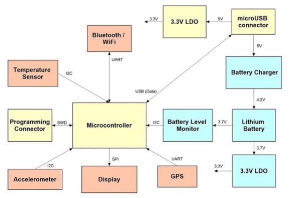
Explain The System Block Diagram

Block diagram of an electronic device showcasing the connections and interfaces between a microcontroller and various components such as sensors, communication modules, display, gps, and power management units.

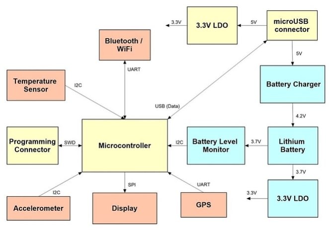
Choose a Production Component.

The intended uses and intended retail price of your device will determine the microchips, sensors, displays, and connectors to use in its creation. You will then be able to draft a Bill of Materials (BOM) thanks to this.

Create The Schematic

Using the system block diagram you produced in step 1, generate the schematic circuit diagram.
The schematic includes all the information needed to assemble the electronics, including information on how each part is related to the others.  

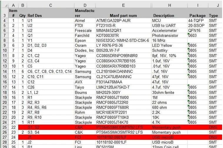
There will be a final Bill of Materials (BOM) that includes information on each electronic component.

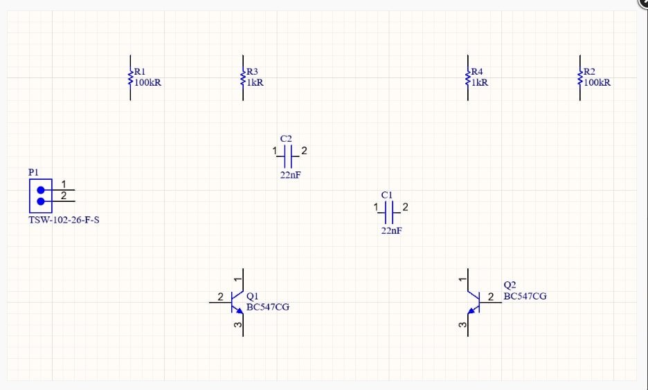
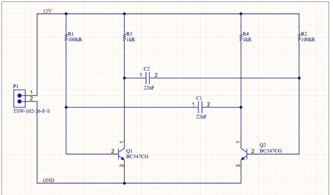
Designing a multivibrator

a diagram of a circuit board

Placing the Multivibrator Parts

The Multivibrator circuit will be assembled using components that were obtained from Manufacturer Part Search using the Components panel. The schematic ought to resemble the picture below when the components have been assembled.

a diagram of electrical components

Netlabels and wiring 

You can use Net Labels to assign names to significant nets in the design, making it easier to find them. As indicated below, you will identify the 12V and GND nets in the multivibrator circuit.

a diagram of a circuit

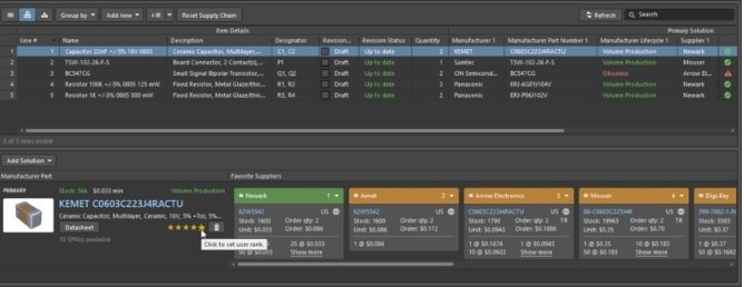
Setting Up the Bill of Materials

In the end, comprehensive supply chain data must be included for each component used in the design. You can add this information in an Active BOM (*.BomDoc) at any time during the design cycle, instead of having to add it to each design component or as a post-process in an Excel spreadsheet.

a screenshot of a computer

Conclusion 

Through the use of standardized symbols to express component connectivity and interactions, circuit schematic diagrams offer a fundamental depiction of electronic systems. creating schematics. The bill of materials is essentially the lifeblood that synchronizes the whole manifestation of a complicated PCB assembly from first conceptions into a tangible product; it is much more than just an ordinary parts list. It offers best practices and advice for producing a high-quality design in addition to covering the fundamentals of schematic capture and the regulations that must be adhered to throughout PCB routing. The industry standard tools and software for schematic design are also covered in the guide. Whether you are new to PCB design or looking to advance your knowledge, this guide offers helpful advice and information for creating printed circuit boards of the highest caliber.

PCB Runner team has an experienced team of development & simulations team which can make schematics & BOM for customer base don input & output requirements. Feel free to reach out to our team at sales@pcbrunner.com & engineering@pcbrunner.com

pcb prepregs

Core/Prepreg Thickness

Understanding PCB Cores and Prepregs: Properties, Selection, and Future Trends

Introduction

In essence, PCB cores are one or more prepreg laminates that have been heated, pressed, hardened, and cured. Copper foil is applied on both sides of the core.  The PCB’s isolating substance is called Prepreg Core. Prepreg serves as both a multipurpose inner conduction medium for PCBs and a binding agent. A resin is infused into prepreg material; the resin is not cured but toughened. Consider the prepreg to be the binding agent that keeps the main components together. A prepreg laminate will start to bond to the neighboring layers when two cores are layered on each side then heated and compressed. The crosslinking process of the hardened resin gradually cures it, bringing its final material qualities closer to those of the core layers.

There is a glass weaving in the resin substance. Using a loom, the weave can be made tight (7628 prepreg, for example) or loose (1080 prepreg, for example) during production. The final product’s electromagnetic properties (dispersion, losses, and any fiber weave effects observed by signals in the board) are determined by the gaps and homogeneity of the glass weave.

Prepreg Thickness

Prepreg in PCBs 

Insulation is the primary function of prepreg in PCB construction. It is a layer of building material that sits between the inner core and the copper surface of a board. Its function is to operate as a dielectric substance between these layers to stop current flow. It is frequently referred to as a binding substance and is utilized to help strengthen a board because of the way it is linked between these layers. A prepreg layer can be modified in a variety of ways by the client, such as adding chemicals and catalysts to make it more conductive or to boost insulation.

Since prepreg is made of fiberglass cloth coated in a resin reserve, it is simple to attach to core material. Glass strands are knitted together to create a glass tissue, which is then given time to partially dry. It acquires an adhesive characteristic when it is pasted over the core substance. Designers monitor the material’s volume friction prior to adhesion because it will ultimately decide the prepreg layer’s final characteristics. This is the point at which manufacturers modify it to satisfy client specifications. Thankfully, this versatility implies that a wide range of prepreg materials can be found to satisfy practically any requirement. It’s a terrific extra skill because of its easy application and mastery. Additionally, the weight of a board can be decreased by adding a prepreg layer, which makes board design downsizing easier.  

PCB core 

Both single-sided and double-sided PCBs are built using a core. The base upon which we build the entire board is known as the core material. It’s a solid plate that you may coat with copper (and Prepreg for insulation) on one or both sides.  An FR-4 (Flame Retardant) mixture of components, including copper traces and titanium epoxy laminates, make up a core. It is woven with fiberglass fabric to produce a solid surface that resists fire. After that, copper is applied on both sides of it to create the PCB’s foundational material. By itself, it produces a stable, pliable surface that can be used to assemble parts. Its strength significantly rises with a prepreg layer without adding a lot of extra weight. To build multilayer PCBs, the majority of electronic manufacturing services mix the two.

Properties of PCB Prepregs

Qualitative characteristics in prepregs for superior PCBs:  

Dielectric Constant: Low dissipation factor and stable dielectric constant are necessary for high frequency performance. 3.5–5 values are normal for prepregs made of glass fiber and epoxy.  

Low Z-axis shrinkage and expansion during temperature cycling prevents via failures and is a sign of dimensional stability. X-Y shrinking often less than 0.5%.  

Bond Strength: Excellent resistance to delamination and strong adherence to prepreg layers and copper foils. Strength of bond > 2.5 N/mm.  

Decomposition Temperature: A high Td above 300°C minimizes charring problems and indicates stable thermal performance.

Moisture Absorption: Low affinity for moisture guards against vapor pressure-related reliability problems and electrical leakage. Uptake standard <0.5%.  

Flow and Filler: Sufficient resin flow to cover defects, but not too much to prevent wire shorts. Filler loading ranges from 15% to 40%.  

High level of resistance to burning, igniting, and producing smoke is known as flame retardancy. Material certified UL 94 V-0.

Properties of PCB core

1) Thermal characteristics  

The amount of heat that a substrate can tolerate is determined by its thermal property. The whole PCB’s heat tolerance level is determined by the substrate’s heat tolerance levels. Furthermore, the PCB’s heat conduction levels are determined by its thermal characteristics. 

Glass Transition Temperature (Tg): 

Temperatures over a specific threshold cause a PCB substrate to soften. After being taken out of the heat, the substrate hardens back to its original state. The glass transition temperature (Tg), expressed in degrees Celsius, is the range at which a substrate can undergo this transformation. 

Decomposition Temperature (Td): 

A PCB substrate will break down if it is subjected to temperatures over a particular point. The PCB loses five percent or more of its total mass throughout this procedure. Decomposition temperature (Td), expressed in degrees Celsius, is the range of temperatures where this process takes place.

Coefficient of Thermal Expansion (CTE): 

The CTE of a PCB is the measure of its rate of expansion. Parts per million (ppm) is a measure of a substrate’s CTE, which increases when the material is exposed to temperatures over its Tg. Generally speaking, a substrate will have a higher CTE than a copper layer.

Thermal Conductivity (k): 

A PCB’s capacity to conduct heat is measured in watts per square inch. The PCB’s capacity to transfer heat is closely correlated with a material’s thermal conductivity. The amount of heat transfer will be low if the k-level is low, and vice versa. At Kelvin (K), thermal conductivity rates are expressed in watts per meter (W/M).Many dielectric materials have a thermal conductivity range of 0.3 to 6 W/mk. In contrast, the k-level of copper is 386 W/M-ºC. As a result, in a PCB, the copper layer transfers heat more quickly than the dielectric.

pcb prepregs

2) Electrical Characteristics  

The electrical conduction in the PCB is one of the substrate’s electrical properties. Signal propagation speed between components is determined by electrical characteristics. The electrical characteristics of a PCB substrate impact and define several aspects such as bandwidth and signal transmission speed.

Dielectric Constant or Relative Permittivity (Er or Dk): 

Impedance and signal integrity are two of the key elements that affect a dielectric constant’s electrical performance. A PCB material’s relative permittivity (Dk), also known as its dielectric constant (Er), typically ranges from 3.5 to 5.5. 

Tan δ or Df, the Dielectric Loss Tangent or Dissipation Factor: 

 indicates how much less power a material loses when its loss tangent is small. Materials used in printed circuit boards typically have a dielectric loss tangent (Tan δ) between 0.02 and 0.001.Volume Resistivity (ρ): A dielectric material’s volume resistance (ρ) is its resistance to insulation or electricity. High resistance PCB material will not likely facilitate electric charges. Ohm-meters (Ω-m) and ohm-centimeters (Ω-cm) are measures used to determine how resistive a certain dielectric is. A printed circuit board’s material needs to have high resistivity, ideally between 103 and 1010 Megaohm-centimeters, just like all other dielectric insulators do.

Surface Resistivity (ρS): Surface resistivity (ρS) is the resistance of a dielectric medium to insulation and electricity. Similar to the ρ level of a material, the ρS needs to be high, ideally between 103 and 109 cMegaohms per square. Just like ρ, moisture and severe temperatures can affect a material’s ρS level.  

Electrical Potency:

 Electrical strength, expressed in Volts/mil, is a dielectric material’s capacity to withstand an electrical breakdown over a printed circuit board’s Z direction. The electrical strength of the majority of PCB materials ranges from 800 V/mil to 1500 V/mil.

Chemical characteristics 

Chemical attributes include any aspect of a PCB substrate’s chemical makeup. This describes the components of the PCB substrate’s chemical makeup. The toughness of a PCB is determined by its chemical makeup.

Flammability Specs (UL94):
The Standard for Safety of Flammability of Plastic Materials for Parts in Devices and Appliances (UL94) ranks the flame-retardant qualities of plastics, sometimes referred to as plastics flammability, from highest to lowest. UL94’s PCB material standards stipulate that specimens must not burn with blazing combustion for more than 10 seconds. A collection of five specimens cannot burn together with blazing combustion for more than 50 seconds.

Moisture Absorption:
The ability of a dielectric material to tolerate being submerged in liquid is known as moisture absorption. The moisture absorption values of most PCB materials range from 0.01 percent to 0.20 percent.

Methylene Chloride Resistance:
The resistance of a dielectric to methylene chloride absorption is the most direct indicator of a PCB material’s chemical resistance, and it is known as methylene chloride resistance (MCR). The MCR range for dielectrics is typically 0.01 percent to 0.20 percent.

Mechanical characteristics 

A PCB’s mechanical characteristics, such as its substrate’s hardness, plasticity, density, and resistance to corrosion, are used to determine its characteristics. Depending on your PCB’s intended use, the mechanical characteristics play a significant role in selecting the ideal PCB substrate. 

Peel Power:
Peel strength is the ability of the copper and dielectric layers on a printed circuit board to bind. Peel strength is measured on one-ounce-thick copper traces in three different settings during the PCB manufacturing process: after thermal stress, at high temperatures, and after chemical exposure. 

Flexural Strength:
Measured in kilograms per square meter or pounds per square inch, flexural strength refers to a dielectric material’s capacity to withstand physical stress without breaking. A printed circuit board’s flexural strength is evaluated by applying force at the middle, with only the ends supported.

Density:
The density of a dielectric material is expressed in terms of grams per cubic centimeter, or g/cc. Alternatively, pounds per cubic inch (lb/in^3) can be used to express PCB density.  

Time to Delamination:
This phrase refers to the length of a dielectric material’s resistance to influences that cause delamination. It establishes the amount of time that a PCB’s layers will remain separated from one another when exposed to temperatures that above a specific threshold. Any PCB material, including fiberglass and laminate, is susceptible to delamination from heat shock or moisture.

Selecting the Right Thickness for Your Project Requirements

Choices for PCB Thickness: 

The total thickness of your PCB is determined by the number of layers on it. While certain applications call for a thinner PCB, others require a thicker one. Thus, there are wide variations in the thickness norms. The combined thickness of the prepreg and core typically ranges from 0.008 to 0.240 inches.  

Conventional PCB Thickness: 

Single-sided, double-sided, and multilayered PCBs are all possible. The standard thickness, 1.57 mm or 0.063 inches, is a holdover from earlier standards. This is a result of the plywood industry’s use of 0.063-inch plywood sheets as substrates for electrical equipment. However, the thickness range that you can choose from now is 0.008-0.240 inches. The advancement of multi-layer PCBs is to blame for this.

Selecting the PCB Thickness: 

Keep in mind that a thicker board has a lower chance of breaking than a thin one when selecting thickness. It is preferable to stay with a thick board unless the application specifies otherwise. When selecting the PCB thickness, the following considerations should be made. 

  1. Weight: Because a thinner board is more brittle, it will break more easily. Therefore, unless the applications call for a thin board, thicker boards are preferred.  
  2. Flexibility: While thinner boards are more pliable than larger ones, they are also more prone to breaking. Thick boards weigh more and have less flexibility.  
  3. Space Requirement: A thicker board is preferable if your device has enough room for a larger PCB; on the other hand, a smaller board will be needed if your device is smaller.  
  4. Components and connections: A specific thickness will also be needed depending on the kind of connectors and components you choose.  
  5. Impedance: The board’s thickness and impedance must be matched. This is so because the dielectric, which aids in impedance control, is essentially the same thickness as the board.

Electrical Conductivity 

The electrical conductivity and signal quality that flow through the PCB are also impacted by its thickness. Because they have less resistance, thicker PCBs can handle higher current levels without overheating or making noise. Conversely, thinner PCBs can produce more noise and distortion, have more resistance, and worsen signal quality, all of which can impair the circuit’s performance.

PCB Thermal Design Factors

To get you started with addressing the thermal considerations in your design, consider the following design guidelines.
As a general rule of thumb, your board should have an area of 15.3 cm², or 2.4 in², each watt dissipated for a 40°C rise in board temperature in order to dissipate 1 watt of power. This demand can be reduced in half (7.7 cm² or 1.2 in² per watt) if the board is exposed to airflow. These numbers presuppose that the board is positioned to allow free airflow around both sides and that the component is thermally linked to a copper plane that reaches to the board’s corners. An external heat sink might be necessary if these power density specifications are too restrictive for your design. Additionally, a temperature rise of 40°C is a decent place to start when it comes to circuit board temperature control.
a. It is recommended practice to arrange power components on a board so that they heat your PCB uniformly whenever there are several power components present. Significant temperature variations along your PCB design prevent your PCB from efficiently transferring thermal energy away from the installed power components. After a design revision is finished, thermal imaging, if provided to the designer, can enable the empirical inspection of your component location.

b. Your PCB will transfer heat energy to the linked copper plane more effectively the more vias you can put beneath your component. Increase the number of vias in contact with your package’s power pads (the sizable, thermally conductive pads of the component) by using array vias.

c. You will need to utilize larger copper weights in designs that dissipate more energy. For power designs, it is advised to start with one ounce of copper.

d. Tracks that run perpendicular to the thermal path away from the power component must not obstruct the pour of copper when using it to dissipate thermal energy away from a component.

e. It should be noted that if a heat sink is required to maintain the system’s temperature within tolerance, its effectiveness will usually be significantly increased if it is positioned so that it is thermally connected to the component’s case.

Usually, this entails mounting the heat sink on the board’s other side from a surface-mounted component. Although it could be tempting to put a heat sink right on top of the component, the plastic case’s thermal resistance will make the heat sink useless. As previously mentioned, packages specifically intended to have heat sinks connected to their “tops” are an exception to this rule.

Mechanical Strength  

Impact resistance, flexural strength, and tensile strength are important mechanical characteristics to consider. The material’s resistance to bending is measured by flexural strength, whereas its tensile strength indicates how well it can tolerate stretching pressures. Conversely, impact resistance assesses the material’s capacity to tolerate shocks or abrupt impacts. The resistance of your board to breaking or deforming under bending load. IPC-6013C stipulates that stiff, flex, and rigid-flex standards must be followed.

Dimensions: Density (g/cm3): the mass per volume of a dielectric

 Time to Delamination: the length of time a PCB’s layers will stay bonded when exposed to temperature changes or moisture; Peel Strength: the resilience of copper layers and dielectrics under thermal and chemical stress.

FACTORS INFLUENCING PCB PRICES 

The kind of material, the size of the board, and the number of layers are the three variables that have the biggest effects on the breakdown of PCB manufacturing costs. The finish and the size of the holes, including these eight, are further considerations that can affect the cost.  

 Selection of Materials 

The cost of a circuit board is always going to depend on the materials that go into it. The FR4 material used to laminate standard PCBs is insufficient for boards intended for high-intensity applications, such those used in the petroleum and aerospace sectors. The selection of materials used affects a PCB’s cost. 

Different materials make up PCBs, and the choice of these materials has an impact on the final cost. The quantity of material used to produce PCBs is also greatly influenced by the size of the circuit board. Costs can be decreased by maximizing the reduction of material utilization. Additionally, when choosing materials, other aspects like mechanical qualities, thermal performance, temperature dependability, and signal performance should be considered.

PCB Dimensions 

 Modifying a PCB’s dimensions and form has a big impact on production costs. The final product will cost more since enlarging the PCB will take more material and time.  As the PCB’s surface area increases, so does its cost, thus you can figure out how much more it will cost for sizes that are larger than the typical ones. It’s crucial to remember that a PCB’s price is determined by both its overall size and the amount of space that each component takes up.

Quantity and Scale: 

The cost per unit of PCBs is directly influenced by the quantity produced. Economies of scale are frequently realized in large-scale production and batch manufacturing, which lowers the total cost per PCB. Prototyping and smaller production runs, however, are typically more expensive because of the lower production volumes.

Supply Chain and Procurement: 

The cost of producing PCBs can be affected by the selection of suppliers, the sourcing of materials, and procurement tactics. Saving money can be achieved by maintaining material quality, choosing reputable suppliers with competitive prices, and streamlining logistics and transportation. Additionally, there can be financial benefits to investigating outsourcing choices and forging solid alliances.

Technological Developments and Market Trends: 

Both might have an impact on the price of producing printed circuit boards. The efficiency and cost of production can be affected by the introduction of new materials, industrial processes, and automation technologies. In order to stay competitive, manufacturers may also be compelled to streamline operations and cut expenses due to price constraints and market rivalry.

Important Technologies for High Density PCBs  Several sophisticated processes for PCB fabrication are necessary to produce the high-density boards that are required today:  

Drilling Using Lasers  

The five mil and smaller via diameters exhibited in HDI are not achievable with mechanical drilling. These tiny vias are precisely and tightly drilled using UV lasers. Along with producing cleaner walls, laser technology also prevents smears and epoxy blockage caused by microscopic particles.  

Minimal Dielectrics  

For high speed HDI boards, standard glass fabric substrates are excessively thick and lossy. The popular low-loss thermoset laminates with dielectric thicknesses as low as 25 μm include Teijin’s Nexus and Panasonic’s Megtron 6. They avoid problems with signal integrity and permit tighter lines or spaces.

Direct  Imaging  

Rather than using a mechanical print-and-etch process, photolithographic techniques are utilized to produce ultra-fine traces smaller than 25 microns. Laser direct imaging is used to expose liquid photoresists in order to precisely define the circuit patterns.  

Buried and Blind Through  

Prior to the outer layers being laminated, blind or buried vias are drilled and plated to enable connections between the inner layers without using up routing space. This gives HDI designs a great deal of routing flexibility.

Microvias: 

These are tiny vias drilled using a laser, usually measuring between 50 and 80 μm in diameter. In HDI boards, microvias link neighboring layers without consuming board space.

Assemble layers:

Sequential lamination is used to add more thin dielectric layers on both sides of the core HDI board. In order to reduce congestion and integrate components, these offer additional routing layers. 

 Pitch/Fine Pad SMT  

Fine pitch component packing, with pitches ranging from 0.4 to 0.15 mm, is used to fit more components into smaller spaces. The pad geometries and tolerances required for this must be achieved during the PCB fabrication process.

HDI Board Construction

Three basic HDI board construction styles are utilized: 

  1. Fundamental HDI 

There are four to eight blind via layers in this structure, and microvias connect at least one fine line layer to the top or bottom. Blind vias do not require via stubs because they route across internal layers. Fine pitch SMT components can be integrated using a 25–50 μm finish layer. 

  1. Hard HDI 

Robust HDI boards consist of bulkier sub-assemblies with conventional and blind/buried vias for routing density, sandwiched between very thin core and buildup layers with microvias. Large boards may have several of these sub-assemblies.

     3. HDI for Sequential Lamination

In this case, the core board has six to twelve layers. Next, successive layers of build-up are applied by laminating thin dielectric films ranging from 25 to 60 μm in thickness.  Each layer has stacked vias that create connections between the layers. It is possible to incorporate components in the outer build-up levels. The number of layers, component density, routing congestion, and other design requirements determine which HDI structure is best.

Future Tends:

Technology is always changing, and this is also true in the field of high density PCB design. Future trends to watch out for include the following:  

Future Tends

Miniaturization: 

The need for high density PCBs will only grow as devices get more compact and smaller. In order to fit more components onto smaller boards without compromising durability or functionality, PCB designers will need to get inventive. 

Advanced Materials:

 3D printed circuit boards and flexible PCBs are two new materials that are gaining popularity. These materials have special benefits like greater durability, reduced weight, and enhanced flexibility.

Increasing Automation:

 More PCB design processes are probably going to be automated in the future as artificial intelligence and machine learning continue to grow in popularity. This might result in shorter design durations, fewer mistakes, and more effectiveness.  

Better Testing and Validation: 

With the complexity of high density printed circuit boards growing, it is critical to extensively test and validate designs prior to manufacturing. To make sure that PCBs fulfill the highest requirements for quality and dependability, new methods for testing and validation are being developed.  

 All in all, high density PCB design appears to have a promising future. More advanced automation, new materials, and enhanced testing and validation methods will enable designers to produce PCBs that are more compact, robust, and powerful than in the past.

Conclusion 

As this guide has demonstrated, there are some obvious and straightforward distinctions between Prepreg and Core. Overall though, they cooperate to guarantee that your PCB performs at its best. Choosing the correct partner is crucial when deciding between Prepreg and Core. Both require the dexterity of seasoned pros.  Our primary goal at IBE is to work together with you to achieve your goals and objectives. You can visit IBE electronics for additional content and details. Our comprehensive understanding of PCBA guarantees that we will competently fulfill your demands. Please contact us, and we’ll make sure you receive the most assistance. Prepreg is the basic dielectric component of multilayer PCBs, providing mechanical robustness and electrical isolation of the conducting layers. The PCB’s thermal, electrical, and reliability performance is determined by the makeup of the prepreg, which consists of resin, fabric reinforcement, and fillers. PCB manufacturers can choose the best prepreg material for their process compatibility and performance needs from a variety of prepreg kinds. Strict prepreg handling procedures and quality control methods also reduce variability and guarantee reliable outcomes during PCB construction. Enabling PCB downsizing and dependability requires careful engineering of the prepreg materials as they work at higher frequencies and temperatures and get thinner.

PCB Runner engineering helps industry design layout engineers to propose the working Stack up based on their base material requirements. Do reach out to our team for any questions about stackups & materials at engineering@pcbrunner.com or sales@pcbrunner.com


PCB Panel Design Tips – A Complete Guide

A PCB panel, which is often referred to as a PCB array, is a single board made up of several separate boards. During the breakout process, the constructed panel is disassembled, or depanelized, into the constituent PCBs. Defects are reduced as a result of printed circuit board penalization since automated assembly machines typically have fewer issues during assembly.

 PCB panel design tips

Furthermore, penalization lowers costs by increasing throughout boards. Several design parameters, particularly those pertaining to penalization techniques, are necessary for PCB penalization to be successful. In this collection of penalization rules, we’ll go into further detail about different PCB panel technologies and their particular requirements.

Optimizing for Fabrication: Considerations for Penalization Success

There are several penalization techniques, each with advantages and disadvantages of its own. Which penalization technique is most appropriate for a given application can frequently depend a lot on the layout of the board design and the PCB panel itself. Among these, the following stand out:

Design: The board’s design has the biggest influence on whether penalization technique is best. Certain methods may be far less appropriate than others depending on the clearance between components and the board edge and whether or not there are any edge-hanging or right-angle components.

PCB panel design ideas

Components: The kinds of components utilized on the board are equally crucial as where they are positioned. The best breakout and penalization technique may depend on some particularly delicate parts and connections.

Effective PCB panel design tips

 Materials: The best penalization technique may be limited by the materials used in a PCB since certain materials are more likely to split during the breakout process. The thickness of the board also matters because thin boards are more prone to break during assembly, while larger boards can cause more issues during the breakout process.
These elements restrict the options that each application can choose from.

Currently, only few penalization techniques are widely used out of the three available. They are as follows:

1. V-Score Panelization: Individual PCBs are separated using V-shaped grooves in this popular penalization technique. Using an angled blade, these grooves take out about a third of the board’s thickness from the top and bottom. Since hand-breaking can strain the PCB and nearby components and the remaining third of the board is surprisingly strong between the grooves, a machine is typically utilized to complete the breakout operation.

2. Panelization via Tab Routing: PCB arrays that are not feasible to utilize a V-groove technique will instead employ a tab routing technique. PCBs are pre-cut from the array using this technique, and perforated tabs hold the PCBs in position on the board. These perforation designs frequently have three to five holes. Because this technique may accommodate designs with components that hang over the edge, it is frequently advantageous. As an alternative to using tools, it can also be broken by hand.

For the majority of applications, V-Score and Tab Routing are the recommended penalization techniques. For PCB designers, knowing which of the two approaches is appropriate for their application is crucial. Designing their array for maximum strength and breakout success is the next stage. When feasible, many people use the V-groove Panelization approach due to its effectiveness and decreased surface tension. For this kind of array, depaneling equipment is likewise reasonably priced and economical. Better still, they need little upkeep and are portable. Even though the technique typically produces board edges with more roughness, applications that use V-groove panelization rarely worry about this. V-groove penalization is better for a number of applications, but it has limitations when it comes to PCB panel design. For instance, designs where elements are positioned too near to or dangle over edges are not the best candidates for V-groove Panelization. Additionally, they present a number of production issues that need to be considered when designing, like:

3. Clearance: A minimum of 0.05 inches of space must be kept between components and any V-grooves to prevent damage to components during the cutting process. In order to prevent the cutter from interfering with taller components, it might be necessary to move them farther away. For instance, multilayer ceramic chip capacitors surface-mounted must be spaced from the score line by at least 1/8 inch. Larger connection area components should also be positioned further away from the V-groove because solder junctions can break under the strain of depanelization if they are positioned too close to the groove.

4. Jump-Scoring: When a PCB array is run through a wave-solder machine, V-grooves can weaken its structural integrity and cause the leading and trailing edges to droop.

Designers can add jump scoring to the array’s leading and trailing edges to fortify it and avoid these problems. One approach to achieve this is to run the V-groove about halfway through the leading and trailing array edges and add an ½ inch breakaway edge on each. Simply tell those who operate the depaneling machines to take off these breakaway edges before separating the boards. A V-scored panel should have a few issues during the manufacturing and assembly process if these design factors are considered.

DESIGN CONSIDERATIONS FOR TAB ROUTING PANELIZATION

Panelization with tab routing is typically chosen in applications where components are positioned very near to or above edges. It’s also better for PCBs that are shaped like circles or other non-rectangular geometries. To guarantee the strength and operation of these arrays, particularly during the breakout process, a number of design decisions must be made because the tabs serve as the arrays’ breaking points. Among these things to think about are:

1. Clearance: Keep parts and traces at least 1/8 inch away from the tabs due to the stress at the breakaway points and the possibility of splintering. To ensure the least amount of interference, surface-mounted multilayer ceramic chip capacitors need to be placed further away from the tabs—at least ¼ inch.

2. Knock-Outs: To avoid problems during the wave-solder process, a placeholder, or knockout, may be necessary if your PCB design contains holes larger than 0.6 inches. Since PCB panels are more likely to sag in the middle of an array, knockouts are especially crucial there. Larger, more irregularly shaped knockouts could require numerous three-hole perforated tabs, whereas smaller rectangular knockouts can have a wide, five-hole perforated tab on a single edge.

3. Tab Positioning: To keep your PCB array design intact, tab positioning is crucial. For five-hole perforated tabs, tabs must be spaced every two to three inches around the edge of the board; for three-hole perforated tabs, tabs must be spaced every 1.5 inches. To prevent curvature at the board edge, tabs should be positioned as close to the edge as feasible; nevertheless, they shouldn’t be positioned beneath protruding parts. In addition, the designer needs to make sure the tabs are large enough to hold the boards in place without getting in the way of the breakout procedure.
Place Perforations: Never run tab perforations in the middle of a tab if you want to prevent protrusions from the side of your board. Instead, run them near the edge of the PCB, or on each side if the tab is positioned between two PCBs.

4. Array Layout: To ensure that there are uniform break-lines across the array, make sure that all tabs that are broken at the same time are collinear when assembling PCBs. Benefits of Panelization for PCBs
In addition to making smaller boards fit into conventional production procedures, PCB panelization increases production efficiency.

Typical benefits of PCB panelization consist of:

1. Production in bulk: Panelization is a time and cost-effective solution if you have a large number of boards to produce. product security: The PCB is shielded from vibration and stress during assembly by panelization.

2. Swiftness and effectiveness: Processing several boards simultaneously as part of a huge array is quicker and more effective for tasks like paste printing, component assembly, soldering, and even testing. Inconsistent break-lines can cause tabs to break in some cases and drag tabs perpendicular to the board surface in others, tearing the lamination.

If you keep these things in mind, you should have a few problems with your design when it comes to manufacturing and breaking out. Panel sizes that are standard. Manufacturing boards with the fabricator’s standard processing panel is frequently more economical. Although every manufacturer has different preferences when it comes to panel sizes, 18 x 24-inch panels typically have an ½ inch perimeter of clearance for handling double-sided boards and an inch for multilayer boards. Before writing a panel for your fabricator’s assembly procedure, you should consult with them.

Common Pitfalls and How to Avoid Them:

A PCB panel’s successful and cost-effective design depends on adhering to a few crucial rules of thumb:

1. PCB Panel size

Pick-and-place, solder past printers, quality inspection machines, and other machines in the printed circuit board production chain often specify the range of panel sizes that can vary (AOI). Because of the conveyor width, panels smaller than 2 inches, or around 50 mm, cannot be processed. Either more PCBs need to be placed on the panel or open areas around the edges need to be provided in order to prevent this issue. On the other hand, the machines also establish the panels’ maximum dimensions. The maximum dimensions for the majority of models line up with common panel sizes, like 9” x 12”,  12″ x 18″, 18” x 24”

2. Type of PCB panel

Particularly flexible, but many stiff PCBs also feature irregular and non-linear curves because they must fit within the installation space constraints. However, the panels need to have two parallel and straight edges in order to be transported by conveyors and to make handling easier. Consequently, the uneven curves require the addition of an otherwise unused handling edge (seen in the illustration as light green). Since saws and milling machines, for example, have severe constraints regarding their geometric flexibility, the panel’s design also makes it possible to draw inferences about the cutting procedure to be utilized.

3. Distance of PCBs and spacing of cutting edges for components

Depending on the separation technique used, the minimum distances between the individual circuit boards that need to be maintained can change dramatically. For example, the channels themselves are merely a few millimeters broad after milling. In contrast, the distances can be reduced to a minimum of a few hundred µm with laser depaneling. In general, these savings allow for a large increase in the number of PCBs per panel, especially with microscopic dimensions. Not only must the distances between the PCBs be taken into account when separating the circuit boards, but also the distances from the cutting edge to the mounted components. In this instance, the component heights in particular are crucial. Greater spacing must also be kept as a general rule for higher components on the circuit board. Even in this instance, the tool and cutting technique will determine which distances need to be taken into account. This is another area where space on the panel can be saved, as the laser beam is much thinner than a milling head or saw blade. Generally speaking, even delicate parts can be placed roughly 100 µm away from the cutting edge without experiencing heat or mechanical stress.

4. Full cut of PCBs

Another way to separate the circuit boards is to cut them without using any kind of tabs or V-grooves as a pre-process. Given that the width of the cutting channel and cutting tool play a crucial role in the so-called full cut of the PCBs, laser depaneling in particular provides a number of benefits. As an illustration, the milling machine needs a cutting channel between 2000 and 3000 µm in width, whereas the laser beam only needs one that is roughly 200 µm wide.

This gap allows for a significant increase in the number of PCBs per panel, particularly for smaller PCBs and larger panels.

Read More: Differences between Counterbore and Countersink

Conclusion

It has been demonstrated that the panel’s design is a challenging undertaking that requires careful consideration of several important variables. These significantly affect the PCB production’s cost, quality, and profitability. Specifically, selecting the right separation method is crucial to the design and optimal panel utilization. In this case, mechanical processes are linked to notable constraints.

FAQs

Q1: What are the benefits of doing Panelize PCB during design layout?

The benefit of the printed circuit board panelization process is a decrease in defects as automated assembly machines tend to encounter fewer problems during the assembly process. In addition, panelization also reduces costs by improving throughput.

Q2: Basic points need to be ensured while proposing a PCB Panel.

PCB designers should consider the following points while panelization :

Overhanging Components:

Additional space must be allowed around the board outline in the PCB panel for components, such as connections, that protrude above the board. You should first discuss all of your alternatives with your manufacturer as this may have an impact on the panel’s design.

Tooling Holes and Fiducial Marks:

These are elements that your manufacturer will incorporate into the panel; ensure that your placement does not result in any issues.

Component Weight:

If there are a lot of components together, the PCB panel may bend and more support would be needed. You can first inquire about any helpful PCB layout alternatives by speaking with your manufacturer.

PCB Width:

A PCB panel may potentially bend as a result of thin circuit boards. When the panel bends while passing through the wave, this may cause issues like solder to spill over the top of some of the boards. Your manufacturer might have to use a pallet or brace the board as a result, which could affect where you arrange your components.

Why Us?

PCB Runner offers a proposed array based on the individual board requirements, we make it less hassle for the layout designer to step & repeat the PCB and supply us with panelized Gerber. Submit your Gerber files at https://www.pcbrunner.com/free-pcb-quote/ or do reach out to our team offline at engineering@pcbrunner.com or sales@pcbrunner.com for your current or upcoming project’s needs.

PCB Standard & Heavy Copper Thickness

A new trend in the printed circuit board business, Heavy Copper, and Extreme Copper Printed Circuit Boards, is being tapped into by an increasing variety of power electronics products. The majority of PCBs that are sold commercially are made for low-voltage/low-power applications, and their copper traces and planes are composed of copper weights that range from 1/2 to 3 ounces per square foot. Copper weights for a hefty copper circuit can range from 4 to 20 ounces per square foot. Extreme Copper refers to copper weights that are above 20 oz/ft2 and can reach up to 200 oz/ft2. We’ll be talking mostly about heavy copper thickness.

Heavy copper thickness in PCB manufacturing process 

Standard printed circuit boards are created by combining copper etching and plating techniques, regardless of whether they are double-sided or multilayered. Initially, circuit layers are made of thin copper foil sheets (usually 0.5 to 2 oz/ft2) that are etched to remove excess copper and then plated to give planes, traces, pads, and plated-through holes more copper thickness. The circuit layers are assembled into a comprehensive package by laminating them onto an epoxy-based substrate, like polyimide or FR4.

The production process for boards with heavy copper circuitry is the same, but specific etching and plating methods, like differential etching and high-speed/step plating, are used. In the past, thick copper-clad laminated board material was totally etched to create heavy copper features. This resulted in uneven trace sidewalls and unacceptably high undercutting. The combination of plating and etching has made it possible to manufacture hefty copper features with straight sidewalls and minimal undercut because to advancements in plating technology.

The Advantages of Heavy Copper PCB

  • Better thermal performance: During the manufacturing and assembly procedures, heavy copper printed circuit boards (PCBs) can tolerate numerous temperature cycles.
  • Greater current carrying capacity: PCBs made of heavier copper have larger current capacities and better electrical conductivity. The current carrying capability can be increased by widening the copper trace, and even higher current loads can be supported by thicker copper traces.
  • Enhanced mechanical strength: PCBs made of heavy copper have stronger connections and plated-through holes, which guarantees the board’s structural integrity and increases the electrical system’s resilience to voltage.
  • Outstanding dissipation factor: PCBs made of heavy copper work well with big power-loss components. These PCBs have the ability to efficiently disperse heat and stop electrical systems from overheating.
  • Good conductor: Heavy copper PCBs are useful in the manufacture of electrical items because they are good conductors. They assist in joining different boards so that currents can be transmitted.

Applications for PCBs Made of Heavy Copper

Because heavy copper PCBs are widely used in the following industries, their popularity is growing:

  • Military: Radar, weapon control, and surveillance systems.
  • Rails Tracking: Rail track system and signal transmission system for the automotive sectors.
  • Power distribution: High power rectifiers, power grid switching systems, overload relays, and excitation systems for power regulators.
  • Transportation: Traction converters, power line monitors, and power converters for railroad systems.
  • Industrial controls: Surge protectors, protection relays, welding equipment, safety, and signal systems. 
  • Renewable Systems: Control panels for hydroelectric power facilities, energy storage, power grid backup, and power converters.

 Services offered by PCB Runner include PCB Assembly (SMT), Electronics Module Sales, CNC Machining, PCB Prototype & Batch Production, and more. We are dedicated to satisfying the demanding demands of international manufacturers across many industries with regard to electronics quality, delivery, affordability, and other matters.

Heavy Copper Thickness PCB Design Guidelines

The following are some important design factors for PCBs made of heavy copper:

Layer Assembling

  • To reduce warpage, place thick copper layers close to the board’s core.
  • Avoid positioning outer layers adjacent to one another as this can worsen registration problems.
  • For stability, rotate the direction of the fiber weave by ninety degrees between neighboring dielectric layers.

Part Location

  • To ensure solder mask coverage, make sure there is enough space between plane layers.
  • Take into consideration component shadows that fall on inner copper layers.
  • Inspect drilled holes for exposed copper.

Temperature Control

  • To serve as heat spreaders, place heat-generating components on top of thick copper layers.
  • Provide many vias to distribute heat to the interior planes underneath heated components.
  • Elevated Current Pathways
  • For high-current lines, use copper pouring or polygons rather than routing several parallel traces.
  • For heat dissipation, place next to plated thru-hole vias.
  • The use of filled vias should be restricted since, in comparison to hollow vias, they hinder heat transfer.
  • Solder masks should be kept free of holes and countersink-filled vias.

Panel and Tooling

Give ample room for manufacturing and assembly tolerances. Consider warpage, stretching, and shrinkage of the cloth. For simple tooling, use fiducials and test coupons on the panel.

DFM Evaluation

During the design phase, ask the fabricator for DFM feedback.

In particular, look into manufacturability with regard to heavy copper tolerance concerns.

Getting in touch with the PCB maker early on streamlines the design process and helps to prevent problems during the prototype.

Finding the Right Heavy Copper Partner

Make sure the PCB manufacturer you choose for your heavy copper boards satisfies the following requirements.

Checklist of Capabilities

  • Lamination thicknesses of 2 oz, 3 oz, 4 oz, and so on are available.
  • PTH filling: epoxy plugs, conductive ink, and copper
  • Preferred registration accuracy is ≤ 0.003″.
  • Etching with fine lines: < 4 mil line/space
  • The thickness of plating: ≥ 2.5 mils copper in holes
  • Gaps to be filled by sectional plating after etch AOI examination – 5+ high-resolution cameras.

Standards and Licensure

  • Shop floor processes in accordance with IPC 6012 Class 3
  • ISO 9001 certified
  • UL or TUV-approved facilities
  • Qualification testing- vibration, shock, and thermal stress

Technical Proficiency

  • Familiarity with intricate copper designs
  • Support for Design for Manufacturing (DFM)
  • Simulated plane currents and thermal analysis
  • Comments on dependability, stacking, and layout

Active Prototyping

  • Minimal NRE expenses
  • There are no minimum order requirements.
  • Compact panel or array sizes
  • Simple 2-4 layer constructions can be completed in 24 hours.

Examine manufacturers carefully based on these factors prior to selecting your heavy copper PCB supplier.

Read More: PCB Component Placement Guide – Everything You Should Know For Effective PCB Assembly! 

Conclusion

Applications with large current loads, demands for thermal performance, and requirements for power integrity are made possible by heavy copper PCB technology. Although the thick copper layers increase reliability, strict process controls are required during fabrication. The benefits of heavy copper PCBs in your product can be realized by closely collaborating with the PCB manufacturer throughout the design phase and adhering to layout specifications. Heavy copper fabrication calls for specific accuracy and knowledge, thus working with a reputable manufacturer that offers design reviews and qualification testing yields the best results.

FAQ’s

When is the high copper thickness required?

Applications that need power conversions, thermal dissipation, high power distribution, and planar transformers require PCBs with high copper thickness.

Are there any trace width & and spacing restrictions while using high coppers?

High signal count parallel buses or very fine pitch BGAs are examples of PCB footprints used in high-density designs that may call for trace widths as thin as 2.5 mils and unique via types such as laser-drilled micro-vias with diameters of no more than 6 mils. On the other hand, some high-power designs may call for thicker ounce pours than usual and very big traces or planes that consume a complete layer. Applications with limited space may call for extremely thin boards with multiple layers and a half-ounce (0.7 mil) maximum copper pour thickness.

Can high copper traces impact power noise?

Copper traces on PCBs are crucial. Heavy copper can be used to narrow the track width in high-power printed circuit board production while maintaining the same current capacity. The circuit board’s area of occupancy decreases with decreasing PCB track width. In addition, copper busbars for high power and high current can be welded to PCB pads. 

Why Us?

PCB Runner offers Heavy copper clads manufacturing based on high current design requirements, we provide reliable & good quality circuit boards and maintain the required high voltage calculations. Submit your Gerber files at https://www.pcbrunner.com/free-pcb-quote/ or do reach out to our team offline at engineering@pcbrunner.com or sales@pcbrunner.com for your current or upcoming project’s needs.


Difference between Counterbore and Countersink

The goal of both counterbores and countersinks is to enable the head of a screw or other fastener to rest flush with or slightly below the surface of the material they are placed into. The angle at which the bigger hole is drilled separates them from one another. A counterbore is drilled straight into the material, leaving a level bottom between it and the narrower inner shaft, while a countersink’s bigger hole tapers at an angle.

Counter Bore

Except for a handful, the information required for each class is nearly the same. Since a counterbore is always drilled straight down without a taper, the angle is not necessary to know.

counterbore and countersink bits differences

Countersink

We need to know the intended angle because a countersink is not drilled straight into the material. For those who are interested in mathematics, you have probably noticed that the angle and the major hole diameter make a triangle. The angle, major, and main diameters dictate the depth to which the countersink will be drilled, yet stating your anticipated depth is a useful way to verify your expectations.

  • Which way around is the sink on the board? Above or Below?
  • Is plating or not plating appropriate for the hole walls?
  • The hole’s small inner shaft’s completed diameter. (First Drill)
  • Major Diameter: the hole’s final surface diameter
  • The tapered drill’s angle.
  • Depth at which the countersink should be drilled.

Differences between counterbore and counterskink drills in PCB

Important Distinctions Between Counterbore and Countersink Holes

Although hardware can be positioned flush on the board surface with both hole types, there are some significant variations that affect how they are used:

1. Shape of a Hole

The form of the hole is the main distinction. Counterbores have straight cylindrical walls, whereas countersinks have conical shapes. This affects the fastener’s flushness against the board.

2. Size of Top Opening

In a similar vein, the two holes differ in the size of the top opening. A countersink’s top taper gradually from the entire hole width. A counterbore is matched in diameter to the fastener and has a broader concentric cut on top.

3. Walls That Are Vertical

Counterbores have vertical walls, and countersinks have inclined side walls. Fasteners have greater shear strength when the walls are vertical.

4. Width of Bottom Opening

A counterbore’s bottom hole aperture is larger than a countersink’s of equivalent size. This increases the design’s versatility in terms of fastener size selection.

5. Material Elimination

In order to make a countersink, more material is removed from the PCB. Counterbores preserve the strength and substance of PCBs.

When to Use PCB Counterbore and Countersink?

Now that we have a fundamental understanding of counterbore and countersink holes, let’s examine their applications in printed circuit boards.  These fittings can be used on a printed circuit board, even though they are typically meant for stronger materials like metal and wood.  A PCB has holes, just as most circuit boards, and how each hole is drilled counts.
 There are screw holes in some of these holes that are utilized to attach the PCB to an application.
 The sort of screw you can use to drill countersunk or counterbore holes into the PCB depends on what kind of screw is available. Instead of saving space or choosing a smoother design, use counterbore holes if you need a more stable PCB installation.  The screws from them will provide a more stable attachment because these holes are typically big enough to fit socket fixtures.  However, if you’re looking to save space, opt for a countersink hole.

For PCBs, which is better?

Knowing the main distinctions between counterbore and countersink holes is essential to determining when to utilize one over the other during PCB assembly.

The substance you’re drilling into frequently determines which technique you should use. As previously noted, countersinking is frequently recommended when working with wood to prevent overtightened screws from damaging the material.

Most manufacturers will utilize the counterbore approach instead of countersinking during PCB assembly to prevent needless damage to the PCB since countersinking necessitates using an angle and additional depth from the drill. Additionally, countersinking necessitates greater tools and materials, which could prolong the production process and endanger the board.

A ground or earth terminal, which is essentially a physical connection to the earth and serves as a secure return point to drain excess current, can be used to establish a connection through counterboring.  Counterbore holes are also the finest option if you need to mount your PCB more securely. The screws from them will provide a more stable attachment because these holes are typically big enough to fit socket fixtures.

Principal Uses for Each Type of Hole

Countersink and counterbore holes have distinct uses because of their characteristics.

  • Typical Applications for Countersunk Holes
  • Installing flush screws on PCBs’ outside surfaces
  • Allowing low-profile bolt heads that must be flush with the surface of the board
  • Creating a sleek surface for aerodynamics on exposed external PCB layers
  • PCB mounting on thin aluminium covers or panels

Usage of Counterbored Holes in Common:

  • Fasteners for mounting machines that require a high shear strength
  • Letting spacers or washers rest flush against the PCB surface
  • Allowing bigger fastener heads to be accommodated with less material removal
  • Supplying the highest strength possible for screw connections at heavy load
  • Properly assembling internal PCB layers while reducing surface defects

Counterbores offer stronger screw joints, especially for internal PCB layers that are hidden, but countersinks are often better for applications where aerodynamics and aesthetics are important considerations.

Design Factors to Consider When Choosing a Hole Type

Engineers should consider the following aspects when designing a PCB layout and choose between countersunk and counterbored holes:

Sizes of Fasteners

More fastener heads can be used in counterbores than in countersinks of the same size.

Board Space Available

Because of their tapering design, countersinks require extra space.

Location of the PCB Layer

Counterbores work better for internal layers, whereas countersinks maximize outward layers.

Requires Shear Strength

Compared to countersunk holes, counterbores offer stronger screw joints.

Exposure to Environment

For external PCBs, countersunk holes enhance weatherproofing.

Priorities for Aesthetics

The surface finish is smoother with countersunk holes.  It will be easier to guarantee that the hole type chosen offers the appropriate functionality for the application if these factors are considered early in the design process.

 Drilling and completing Compare Counterbored vs. Countersunk Holes

  A functional, dependable PCB requires appropriate drilling and finishing procedures after the hole type has been chosen. The following are some recommended procedures:

Cutting Countersink Holes

  • Use a countersink drill bit that is specifically designed for the screw size. The correct angled hole cannot be created with standard twist bits.
  • To prevent breaking through the bottom layer or tapering too shallowly, precisely adjust the drilling depth.
  • When you get close to the bottom, don’t push too hard to prevent drill walking. Reposition and back off if there is a walk.

How Counterbores Are Drilled

  • A normal straight hole should be drilled first using a twist bit with a minor diameter.
  • Next, cut the shallow counterbore ledge to the required depth using a bigger bit.
  • When counterboring, support the board with a stiff backer to avoid a tear-out.

Finishing  Holes

After drilling, gently deburr the margins of both types of holes to prevent solder mask damage. Further polishing of countersinks with abrasive cones may be necessary to enhance fastener fit.

Proper drilling and finishing will result in smooth holes sized exactly right for the specified fasteners. This eliminates screw damage during assembly and offers reliable performance.

How to take dimensions for a Counterbore and Countersink

To account for the head of the flathead fixtures—which may be bolts, rivets, screws, or other similar objects—the angular sides of a countersink are recessed.

When drawing, the diameter, depth, and included rise of a counter-drilled hole are also provided, together with the surface diameter and angle.  The head of the fastener can rest in the recessed area of the counterbore’s flat-bottomed, cylindrical section.  When drawing and dimensioning this, the diameter, depth, and corner radius are provided and specified. In certain cases, the center can be substituted for the remaining shaft’s thickness when determining dimensions.  Either a rectangular or polar coordinate form could be used to size both holes.

Conclusion

To attach to various materials, counterbore and countersink holes are used with matching screws. It is possible, albeit uncommon, to use this as a print circuit board fixture. As we’ve seen, a counterbore is more cylindrical than a countersink, which is a hole with a cone form. This article has emphasized the distinctions between a counterbore and a countersink, as well as the parallels between them, their definitions, and how both holes function. Since the terms counterbore and countersinks can be used interchangeably, they refer to the same kind of screws that fit into both a counterbore and a countersunk hole. Additionally, we have seen how they differ in their manufacturing process by employing distinct drill bits for every kind of hole.

Why Us?

PCB Runner offers a proposed array based on the individual board requirements; we make it less hassle for the layout designer to step & repeat the PCB and supply us with panelized Gerber. Submit your Gerber files at https://www.pcbrunner.com/free-pcb-quote/ or do reach out to our team offline at engineering@pcbrunner.com or sales@pcbrunner.com for your current or upcoming project’s needs.

 FAQs

  • What minimum angle do we need to maintain for Countersink?

The hardware being used determines the countersink’s angle. Although it doesn’t have to match precisely, the hardware should have at least 50% contact with the countersunk hole. For hardware that is metric, the usual countersink angle is 90°, and for hardware that is imperial, it is 82°. We provide both perspectives in our sizes.

  • Can counter holes be plated for ground connections?

Plated is the best option if the screw is used to ground the board (such as PC motherboards) since it has numerous tiny vias radially surrounding the hole and the top, bottom, and internal ground plane connected together. The vias don’t have any heat relief. The vias make sure that the top and bottom pads are firmly attached to the ground plane, even in the event that the screw thread damages the hole plating. If not, it isn’t really important.

  • Does it cost extra in manufacturing?

However, as Scott Seidman points out, it can increase the cost of the board if there aren’t any other unplated holes in it. The type of lock washer or screw you put on the PCB may depend on whether or not there is a pad and how the pad is finished after assembly because solder has a propensity to flow cold. If the board is multilayer, there should be a lot of space between unplated holes and non-connected internal planes because you don’t want the screw shorting to (say) an internal power plane and the thread can damage the internal surface (people sometimes drill out holes that don’t quite match the mating surface).

Read More: How To Solve The Common Problems During Edge Plating In PCB Assembly? An Expert Guide

The Ultimate Guide to Designing Castellation PCBs for IoT Devices

What are Castellation PCBs?

A particular type of PCB design is known as a castellation PCB (Printed Circuit Board), which has small plated half-holes or notches around the board’s edges. These holes are known as castellation holes, which make it simpler to solder the board and join the PCB to other panels or sections. In surface mount technology (SMT) applications, where components are put directly onto the board’s surface, Castellation PCBs are frequently utilized. This is a typical method for assembling PCBs.

What are Castellated Holes?

Castellated holes are used for setting up an electrical and mechanical connection between two different PCBs or between a PCB and another module. Castellated holes are shaped like a castle’s battlements, with notches or teeth running along their edges. They are placed on a PCB’s edges. It is simpler to solder the PCB straight onto another board or module due to the notched edges.

Why are Castellation PCBs used?

Compact size, multifunction, and high density have increased with the growth of electronic products. The PCBs’ size is continuing to decrease, while the boards’ geometric index is rising daily. Consequently, a change to the soldering procedure is also required. Cold solder will come from using soldering flux to connect the circular hole to the motherboard. The daughterboard and motherboard will have a poorer electrical connection as a result, primarily because of how big the hole is. The electronic device won’t function properly as a result. Thus, the need for plated half-holes is growing every day.

A PCB board’s edges are dedicated to the castellated holes. They may duplicate a PCB circuit’s majority of its components. Assume we have an inverter or filter in our circuit. These little sub-circuits are mass-producible. After that, we may connect them to the main PCB board that carries the circuit’s other components. The castellated holes so copy that specific area of the main printed circuit board.

The following are some applications for castellations:

  • A smaller section of a larger PCB can use castellated PCBs as breakout boards.
  • Castellated holes connect two PCB boards and confirm the solder joint’s reliability.
  • Wireless PCB-to-PCB links can also be created using castellated holes.
  • We can produce integrated modules on a single PCB using this technique. These modules can support additional PCB assembly steps.
  • We are able to customize the component’s pin arrangement to our preference by using these castellated holes.
  • This technique is commonly used with breakout boards or small modules such as Wi-Fi modules.

Types Of Castellation:

Full Castellations:

A printed circuit board (PCB) with its entire edge notched to create a series of extensions resembling a castle’s battlements is known as a full castellation. Because the castellations may be soldered straight to matching pads on the mating board, this design facilitates simple soldering and electrical connections between two PCBs. When a PCB module or daughterboard needs to be safely attached to a main PCB, as in wireless communication modules or sensor boards, full castellations are frequently used. Castellation PCBs frequently use PCB modules to offer extra features and functionality. A printed circuit board (PCB) module is a compact circuit board intended for integration into a larger PCB or system.

Staggered Castellations:

Staggered castellations are a variant of full or partial castellation designs in which the notches are spaced apart along the PCB’s edge. Full castellations are one kind of castellation design. This arrangement can increase the mechanical stability of the joint between two boards since the stress is distributed more equally throughout the solder joints due to the staggered pattern. Staggered castellations are frequently utilized in high-vibration settings or in applications (like automotive or aerospace electronics) where the PCB connection may be mechanically stressed.

Partial Castellations:

Similar to full castellations, partial castellations or half castellations have notches on only a piece of the PCB edge. This arrangement is typically used when constraints on space prevent the use of full castellations or when only certain areas of the board need electrical connections. Applications where a PCB needs to be connected to a flexible circuit, like tiny power supply modules, need for partial castellations.

Mechanisms for Castellation

To maximize the electrical and mechanical performance of the connection, a number of standard configurations can be used in addition to different types of castellations. The choice of castellation type and configuration for use is determined by the particular needs of the application, including the desired electrical performance, mechanical stability, and available space. Each castellation type and pattern has unique advantages and compromises. Among these configurations are:

  • Single-row castellations: Along the PCB’s edge, a single row of notches is made. The most popular and basic design, it can be used for a variety of purposes.
  • Double-row castellations: On the edge of the PCB, two parallel rows of notches are made to improve mechanical stability and boost connection density. When more mechanical support is needed or in high-density interconnects, double-row castellations are frequently used.
  • Interleaved castellations: Each notch in a row is offset from the notches in the row next to it, creating an interleaved pattern in the castellations’ notches. Through a reduction in crosstalk and signal interference between adjacent connections, this arrangement can offer better electrical performance.

Basic Guidelines for Castellated PCBs Holes:

Here are some recommendations regarding Castellated Holes’ specifications. There are various design features that you should consider while using castellated holes for PCB soldering. You need to stick to these qualities while making sure everything is done correctly. The following is a list of suggested measurements for castellated holes:

  • Pad Design: It is preferable to use the largest pad that is available for use. The castellation PCBs fit together correctly when the largest possible is used for each one.
  • Diameter and Distance: Both standard and advanced PCBs use castellated holes. The minimum castellated hole diameter for typical PCBs is 0.6 mm. The castellated holes on modern PCBs should have a lower diameter as possible. There should be a minimum of 0.55 mm between two castellated holes.
  • Surface Finish:  You must carefully consider the surface finishing in order for the PCBs to mount appropriately. For PCBs, ENIG finish can be the ideal surface finish. However, based on how the boards will be used, you can select the finish type that you like most.

Some basic suggestions are:

  • Identify the requirement for castellations in your IoT device.
  • To ensure the correct alignment with the mating board or module, take into account the orientation of the castellated holes.
  • Based on how you solder and assemble the castellations, determine the right size and shape for them.
  • The number of holes on the board is always kept to a minimum when utilizing castellated holes for soldering. Looking for the ideal number of castellated holes can greatly improve alignment and assembly ease. But the number of holes should always match the pattern of the boards.
  • Enough space should be left between castellations during assembly to avoid solder bridging.
  • Choose PCB material that not only supports the castellation’s durability but also satisfies the mechanical and electrical requirements of your application.
  • To avoid unwanted solder connections, apply a solder mask to areas that are not supposed to be soldered.
  • Make sure your PCB manufacturer has clear assembly instructions that include information on solder paste application, alignment, and reflow profile.
  • Carry out the PCB testing procedures, making sure to test the electrical connections’ continuity.
  • Consider the temperature, humidity, and other environmental factors when selecting materials and finishing for your IoT device.
  • Cooperate closely with your PCB manufacturer, keeping lines of communication open and attending to any queries or worries they might have while the product is being manufactured.

You can create castellated PCBs that precisely match the requirements of your IoT device by taking all of these factors into account, ensuring reliable service as well as ease of assembly. To achieve the best performance, the design can be improved with frequent testing and cooperation with experienced PCB manufacturers.

Read More: Soldering Techniques for Printed Circuit Boards (PCBs)

How Castellated Holes are Designed in Altium:

There are a number of ECAD tools in the market to meet the standards of PCB design. Some of them are Allegro, cadence, Eagle, Altium Designer, and Kicad. Altium has a strong and adaptable PCB design tool has support for castellation PCB. Designers may effortlessly generate and enhance castellation patterns, oversee pad designs, and guarantee appropriate inter-castellation spacing with its sophisticated routing and layout capabilities. Additionally, design rule checks (DRC) are integrated into Altium Designer to assist in locating and resolving possible problems prior to manufacturing.

Following are the steps to design single-edge castellated holes as components.

1) Select a pad from a toolbar and place it.

 2) Double-click on the pad and select properties. Now add the following parameters of the pad.

 Hole size=.76mm

 X size= 1.5mm

 Y size= 1.5mm

3) Select a line and place a rectangular region with the following parameters.

4) Now select an arc from the toolbar and place it on the edge of the pad. Select the width of the arc as 1mm.

5) Select all lines along with the arc, go to the toolbar select the following, and convert into a region.

6) Make a solid region and paste the same region into the following layers as it is.

  • Top layer
  • Bottom layer
  • Top solder
  • Bottom solder
  • Top paste
  • Bottom paste

7) One castellated pad is created. Now place it at a distance of 2.54mm and make it a component.

A screenshot of a computer Description automatically generated

You can check it in a 3D view as well.

How Castellated Holes are formed on PCB?

Drilling plated through holes around the board’s edges makes castellated holes. Fabricators must divide the holes along the edge into halves after drilling and then attach the pad to it. The subassembly circuits can be soldered to the main board using these plated semi-holes as soldering pads. These holes are made using a procedure known as side plating or edge plating.

Make sure that there is no gap between the two boards while soldering because it will have adverse effects electrically and mechanically.

Castellation PCBs have many benefits in a range of applications, such as wearable technology, game consoles, consumer electronics, and smart home systems. They are the perfect option for connecting and integrating electronic components because of their small size, simplicity of installation, and enhanced electrical performance. Engineers and manufacturers may optimize their designs for performance, reliability, and manufacturability, eventually improving the end-user experience by understanding the design, manufacturing, and testing procedures involved in generating castellation PCBs.