Surface Mount Technology

How Surface Mount Technology Changed PCB Design Forever

Change is the only constant in technology and electronics. There are many remarkable advancements in the design of printed circuit boards (PCBs); one of them is Surface Mount Technology (SMT). SMT changed the design and machines used to assemble and manufacture PCBs. Knowing how SMT operates and its effects on PCB design will help you understand the reason why it is known as the “game changer” of electronics.

Let us tell you more about what Surface Mount Technology (SMT) is, how it evolved PCB design and its advantages for PCB circuit board manufacturers and designers.

What is Surface Mount Technology (SMT)?

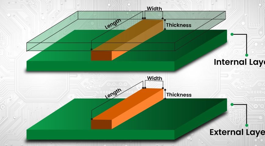
Before there was Surface Mount Technology (SMT), printed circuit boards (PCBs) used to be assembled using a method called through-hole technology. This method uses holes drilled into a board, where electronic components are placed and attached using solder on the opposing side. This technique works, but the large and heavy components required and assembling them was very tedious.

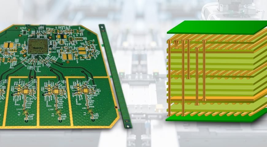
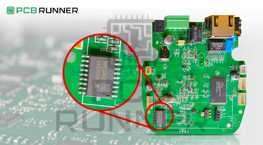
In contrast with SMT (Surface Mount Technology), through mounting techniques, the components are mounted onto the surface of the printed circuit board instead of routed through holes. The elements, referred to as Surface Mounted Devices (SMDs), are smaller in size and are meant to be placed on the top surface of the board. This enables the design of more compact and sophisticated assemblages, leading to adoption by almost all PCB board manufacturers.  

single sided smt and double sided

How SMT Changed PCB Design  

The impact of SMT on PCB design has been transformative, improving speed dramatically and efficiency and making space for more complex circuits. Below are just a few examples of how the landscape has changed:  

1. More powerful miniature devices  

SMT has a greater impact, which is the decrease in the size of components. Through-hole, components were big and bulky, which took a lot of space on the PCB, but with SMT, components are relatively more minor in size, which means more components can be fitted onto a single PCB. This not only led to the development of miniaturized and robust devices like smartphones, too, but also widened the scope of medical equipment.

For manufacturers of PCB circuits, this allows them to produce compact boards that are efficient and advanced in contemporary electronics technology. Also, they save space and material costs.

2. Faster and More Efficient Assembly Process

An improvement in one particular area of PCB assembly is SMT surface mounting technology, which is faster compared to previous techniques. Through-hole assembly, traditionally, every piece was painstakingly inserted into a hole and then soldered individually, which was a tedious and painstaking process.

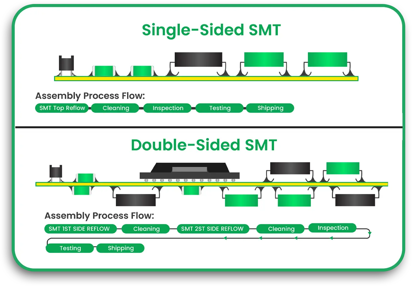
SMT, on the other hand, utilizes automated machines that place the components on the surface of the PCB and not on the holes. Components are held in place by soldering them in a process called reflow soldering wherein the board is heated in a furnace, thus softening the solder paste and adhering the pieces in place. This approach diminishes the amount of manual work required, expedites the fabrication, and enhances the reliability of the results.

Because of the automation potential for PCB customization, custom printed circuit board suppliers experience increased productivity alongside reduced costs.

3. Better Performance and Reliability  

The small size of SMDs and their precise placement on the board automatically enhances the degree of reliability and performance. SMT components are more robust because they have fewer mechanical parts (like leads) that can be subject to wear and tear. Furthermore, the solder joints created by SMT surface mounting technology are more reliable because they tend to have better electrical connections, which strengthens the bond.  

Surface mount devices contribute to an overall decrease in the size and weight of the PCB, thus relieving the stress placed on the board and increasing its mechanical durability. This reduces the likelihood of suffering from failure due to extreme stress.  

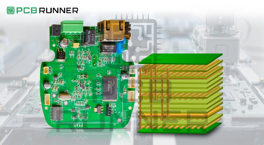
4. Increased Component Density  

The use of SMT enables PCB designers to integrate more components onto the board as sufficed with higher component density. In through-hole designs, components were spaced further apart owing to their larger size. However, with SMT, components can be placed closer to one another, translating to more functionality available in a given space.  

This is extremely useful in the telecommunications industry, where high-density boards are needed. PCB circuit board manufacturers are able to design PCBs using SMT, incorporating more components while keeping the size manageable in view of the powerful and compact devices designed.

5. Cost Efficiency  

Smaller size and faster assembly add cost savings due to the use of SMT surface mounting technology. PCB board manufacturers can accomplish more in less time, resulting in decreased labour and material expenses. In addition, smaller components are usually less expensive than their through-hole counterparts, lowering costs even more.  

Moreover, the use of automated pick-and-place machines means the manufacturer can reduce the use of human hand work in the production process, enhancing resource efficiency and lowering costs. This results in decreased overhead for the production of each board.  

6. Design Flexibility and Innovation  

The invention of SMT has permitted greater flexibility in design. Engineers can custom print circuit boards without as many restrictions as before. The availability of smaller and densely packed components allows for innovative printed circuit board designs which are not feasible with through-hole technology.  

This flexibility enables the production of a broader range of products, from consumer electronics to automotive systems. For PCB board manufacturers, this flexibility means greater challenging designs that can be tailored to client needs.

7. Enhanced Testing and Inspection Capabilities

The Innovations made in Surface Mount Technology (SMT) has also improved the methods used in Testing and inspection of PCBs. Automated Optical Inspection (AOI) systems can effectively and rapidly find errors in surface mount devices. This guarantees that only good and defectless boards come to the higher stage of production.

Moreover, the Standardized geometry and small size of SMDs also facilitate inspection during the production process. This improves yield and decreases the number of defective boards, which benefits PC board manufacturers in the form of savings and increased customer satisfaction.

Key Components of SMT

To analyze the implications of SMT, it is essential to learn the fundamental constituents of SMT surface mounting technology first:

Surface Mount Devices (SMDs): These are the Electronic components that are mounted on the surface of the PCB. Resistors, capacitors, diodes and integrated circuits (ICs) are some common examples of SMDs.

Reflow Soldering: This refers to the process of melting solder and affixing the SMDs onto the board by heating the PCB.

Pick and place machines: These are mechanical devices that position the SMDs on the board in advance of the reflow soldering phase.

Conclusion

Surface Mount Technology (SMT) is a game-changer because it enhances the efficiency of PCB design, reduces costs, improves manufacturing precision, and enables the development of smaller and more powerful devices. Physically Smaller parts, quicker assembly, and better component placement enables the electronics design innovation due to SMT.

For manufacturers of PCB circuit boards, the adoption of SMT surface mounting technology results in more advanced, cost-effective, high-performance PCBs. SMT is now central in fulfilling the requirements of modern technology design for consumer electronics and industrial devices due to the compact, reliable, and efficient design it enables.

SMT will continue to serve as the backbone for advancements in custom printed circuit boards across myriad applications in future and will help professional designers address the challenges of tomorrow.

PCB Trace

How to Accurately Calculate PCB Trace Width

Printed Circuit Boards (PCBs) are the backbone of nearly all modern electronic devices. One of the key components of a PCB is its traces, which are the electrical paths that connect the various components of the board. These traces are responsible for carrying current and signals between components, so it’s crucial to ensure they are sized correctly for the board to function properly.

One of the most essential factors in PCB trace design is the trace width. The trace width refers to the physical width of the copper traces on a PCB. This width must be carefully calculated to ensure that the traces can carry the required current without overheating or becoming too weak to function correctly.

In this blog, we will walk you through the steps of calculating the correct PCB trace width, as well as how to use trace width calculators to make the job easier.

Why Trace Width Matters?

Before we dive into the details of how to calculate trace width, it’s essential to understand why it matters in the first place. PCB traces are made from copper, which is a good conductor of electricity. However, the width of the trace plays a crucial role in determining how much current the trace can safely carry.

If the trace is too narrow, it may overheat due to high current flow, leading to a failure of the PCB. On the other hand, if the trace is too broad, it may take up too much space on the PCB, leaving less room for other components or traces. Therefore, calculating the correct trace width is essential for both safety and efficiency.

Factors That Affect PCB Trace Width

When calculating PCB trace width, there are several factors you need to take into consideration:

  1. Current Carrying Capacity: This refers to how much current the trace needs to carry. Higher currents require wider traces to prevent overheating.
  2. Copper Thickness: The thickness of the copper used for the PCB will impact the trace width. Thicker copper can handle more current so that the trace width can be narrower.
  3. Temperature Rise: The temperature rise refers to how much the trace temperature increases due to the current. You want to keep the temperature rise within safe limits, so you need to adjust the trace width accordingly.
  4. PCB Manufacturer Specifications: Different PCB circuit board manufacturers may have different guidelines or limitations on trace width and spacing. Always check with your PCB board manufacturer for their specifications before finalizing your design.

How to Calculate PCB Trace Width

Now that we know why trace width is essential, let’s go over how to calculate the width of the traces for your PCB accurately. The formula for calculating trace width is based on the amount of current the trace needs to carry, the copper thickness, and the allowable temperature rise. Here’s a simple formula:

W=Ik×(Tr)0.5W = \frac{I}{k \times (T_r)^{0.5}}W=k×(Tr​)0.5I​

Where:

  • W = Trace width (in mils or mm)
  • I = Current (in amperes)
  • k = A constant that depends on the copper thickness (typically between 0.5 and 1.2)
  • T_r = Temperature rise (in Celsius)

While this formula gives you an idea of how to calculate trace width manually, it can be complex and time-consuming. Thankfully, there are tools available to make this process easier.

pcb trace calculator

Using a PCB Trace Width Calculator

Rather than calculating trace width manually, many PCB board assembly companies and PCB circuit board manufacturers provide online trace width calculators to simplify the process. These calculators allow you to input key information, such as:

  • Current (in amperes)
  • Copper thickness (in oz/ft²)
  • Temperature rise
  • Units (mils or mm)

Once you input these values, the calculator will output the optimal trace width for your PCB design. Many online calculators are free to use and can help you save time and reduce the likelihood of errors.

There are several popular PCB trace width calculators available, such as:

  • IPC-2221 Trace Width Calculator: This calculator follows the standards set by the IPC (Institute for Printed Circuits) and provides a reliable way to determine trace width.
  • Online Trace Width Calculator by Advanced Circuits: This free tool allows you to quickly determine the trace width based on the current and other parameters.
  • EasyEDA Trace Width Calculator: This tool is integrated with the EasyEDA design software, making it convenient for designers working with the EasyEDA platform.

By using these tools, you can quickly and accurately calculate the track width required for your PCB design without the need for complex formulas or manual calculations.

The Role of PCB Design Software

When designing a PCB, many PCB circuit board manufacturers and engineers rely on specialized printed circuit board design software to create the layout. These software tools often come with built-in features that can automatically calculate trace width, saving even more time and reducing the risk of human error.

Some PCB design tools that include trace width calculation features are:

  • Altium Designer: One of the most widely used design tools, Altium Designer has an integrated trace width calculator that can help designers select the right trace width based on their design requirements.
  • KiCad: A free and open-source PCB design tool, KiCad offers features to help you determine trace width based on current and copper thickness.
  • Autodesk Eagle: Known for its user-friendly interface, Eagle allows designers to input trace width settings. It will provide feedback during the design process to ensure that the trace width is appropriate.

These tools often integrate directly with PCB fabrication processes, allowing manufacturers to transition from design to production without errors easily.

What Happens If You Get the Trace Width Wrong?

Incorrect trace width can lead to various problems in your PCB. If the trace width is too narrow, the trace may overheat, leading to potential failure. If the trace width is too wide, you may waste valuable PCB space, increasing the size and cost of your design.

In some cases, overly narrow traces can cause a PCB failure during operation. On the other hand, wide traces may contribute to larger board sizes or unnecessary cost increases. That’s why accurate trace width calculation is essential for maintaining reliability and performance.

Conclusion

Calculating the correct PCB trace width is crucial for ensuring the success of your PCB design. By understanding the factors that affect trace width, such as current carrying capacity, copper thickness, and temperature rise, you can make informed decisions about your design. Using trace width calculators and PCB design software will help you save time and reduce errors in your design. Whether you’re a PCB board manufacturer, engineer, or DIY designer, taking the time to calculate trace width accurately will ensure that your PCB works reliably and efficiently.

Make sure to check with your PCB board manufacturer for any specific design guidelines, and always test your designs thoroughly before moving to production. With the right tools and knowledge, you can create high-quality, reliable PCBs that meet your specifications.


PCB Panel Sizes

A Complete Guide to Standard PCB Panel Sizes and Board Dimensions

Want to save money and reduce errors during manufacturing? Start by getting your PCB panel size right. Standard PCB panel sizes help reduce waste, lower fabrication costs, and simplify the production process. Whether you are working with simple boards or high-density interconnect designs, knowing your PCB board dimensions and layout can make all the difference.

IThis blog will discuss standard PCB panel sizes, how to choose the right one for your project, and how this impacts your final cost and board quality.

Why PCB Panel Sizes Matter

When you send your design to a PCB circuit board manufacturer, one of the first things they check is your panel size. A panel is a large sheet that holds multiple PCBs. These panels are then processed as a whole before being separated into individual boards.

Using a standard PCB panel size means your design fits the manufacturing equipment without custom changes. This keeps production smooth, lowers your cost, and avoids waste.

Key Benefits:

  • Maximises board yield per panel
  • Reduces setup and tooling costs
  • Improves material usage
  • Helps meet tight deadlines with less back-and-forth

What Is the Standard PCB Panel Size?

Most PC board manufacturers use the 18 x 24-inch panel as a common size. However, not all of this space is usable. Part of the panel is reserved for tooling holes, test coupons, and routing spacing.

The usable area is usually around 16 x 22 inches, depending on the manufacturer and how they handle margins.

Panel Size Usable Area Notes
18” x 24” ~16” x 22” Most commonly used
12” x 18” ~10” x 16” Good for small boards
21” x 24” ~19” x 22” For large-volume boards

Choosing the right panel size helps balance cost and efficiency. A good pcb fabrication shop will help you plan how many boards you can fit into one panel, called the panelization process.

PCB Panel Sizes


Understanding PCB Board Dimensions

Before you consider panel size, you need to know your individual board size. Most boards are between 2 x 2 inches and 10 x 10 inches, but there’s no strict rule. It all depends on your application and the available space inside the product housing.

Still, there are some points to keep in mind:

  • Boards wider than 12 inches may require custom tooling
  • Tiny boards (<1 inch) often need to be grouped in large arrays.
  • Boards with high component density, like high-density interconnect (HDI) PCBs, might require more panel spacing.

How Board Size Affects Cost

Your board size and how many boards you can fit in a panel affect your final cost. Here’s how:

  • Smaller boards use less material but can be wasteful if poorly penalised.
  • Larger boards use more material but may lower the cost per component due to fewer interconnects.
  • Odd shapes or non-rectangular boards reduce panel efficiency.

That’s why top PCB circuit board manufacturers work closely with you to get the best yield. They use advanced tools and software to calculate the best fit per panel.

Panelization Basics

Panelization is the process of placing multiple copies of your board into one panel. The goal is to make the best use of space, simplify assembly, and reduce waste.

Here’s how you typically penalise boards:

  1. Determine individual board dimensions
  2. Add spacing between boards (usually 0.1 to 0.2 inches)
  3. Add tooling holes and fiducials.
  4. Add breakaway tabs or v-grooves to separate boards later.

Your PCB board dimensions should allow multiple boards to fit neatly inside the usable area of the standard PCB panel size. This helps keep the manufacturing cost-effective and straightforward.

Tips for Efficient Panel Design

To make sure you get the most out of your panel, follow these design tips:

1. Stick to standard dimensions

Stick to standard panel sizes unless your project requires something special. Custom sizes can slow down production and increase costs.

2. Leave enough spacing

Space between boards is needed for routing, panelling, and handling. Too little space increases the risk of damage.

3. Optimise board orientation

Some boards can be rotated to fit more units in a panel. Your PCB fabrication partner can help with this layout trick.

4. Group small boards

If your boards are tiny, consider grouping them into an array to speed up assembly and testing.

What About High-Density Interconnect (HDI) PCBs?

High-density interconnect (HDI) boards are smaller and more complex. To save space, they use micro vias, thinner traces, and more layers. While this means better performance, it also means tighter controls on board dimensions and panel layout.

Some points to consider:

  • HDI boards may need tighter spacing rules
  • Panels need more precise alignment.
  • Standard panel sizes are still used, but yield may be lower.

Work with an experienced HDI PCB manufacturer who understands how to handle HDI designs during panelization and fabrication.

How PCB Manufacturers Handle Custom Boards

Sometimes, your board shape or size doesn’t fit the standard format. That’s okay. Custom boards are common. However, they take more planning. Most pc board manufacturers will suggest:

  • Using a custom panel size
  • Including extra material for support
  • Designing break-off tabs carefully to avoid damage

When working with custom printed circuit board layouts, early communication with your PCB fabrication shop can help avoid problems later.

What You Should Ask Your Manufacturer

When choosing from PCB circuit board manufacturers, make sure to ask:

  • What panel sizes do you support?
  • What is your usable area on the panel?
  • How do you handle odd-shaped boards?
  • Can you help with panelisation planning?
  • What are your limits for high-density interconnect boards?

These questions will help you make the right choice and avoid delays.

Final Thoughts

Choosing the correct PCB board dimensions and panel size might not sound exciting, but it’s a key part of reliable and cost-effective production. Whether you’re making standard boards or working with high-density interconnect, good planning at this stage will save time and money later.

By working with trusted PC board manufacturers and using smart design practices, you can get better-quality boards, faster turnaround, and lower costs.

Key Takeaways

  • The most common standard PCB panel size is 18 x 24 inches.
  • The usable area is less than the whole panel due to spacing and tooling holes.
  • Good penalisation reduces waste and cost.
  • Work with your PCB fabrication partner early to plan the layout.
  • Custom boards may need extra care but are manageable.
  • HDI boards require tight spacing and experienced handling

FAQs

Q: What is the typical spacing between boards in a panel?
A: Usually 0.1 to 0.2 inches, but it depends on routing and depaneling method.

Q: Can I use non-rectangular board shapes?
A: Yes, but they reduce panel efficiency and increase cost. Grouping or rotating may help.

Q: Are there special rules for HDI PCBs in panels?
A: Yes. HDI boards use tighter tolerances and may need extra alignment during fabrication.

Q: Who should plan the panel layout?
A: Your PCB circuit board manufacturer often handles this, but it’s best to collaborate early.

Q: How many boards fit on one panel?
A: It depends on the PCB board dimensions and how well they fit the usable area. A manufacturer can calculate this for you.

PCB Functional Testing

The Importance of PCB Functional Testing and Quality Assurance for Reliability

When you build or buy a printed circuit board (PCB), you want it to work the first time. Whether it is going into a phone, a car, or an industrial machine, your PCB must be reliable. This is why PCB functional testing and quality assurance matter so much. If something goes wrong after the board is assembled, fixing it later can cost time and money. Even worse, a bad board in a critical system can lead to more significant problems. Let us look at why testing and quality checks are a must and how they work.

Why Reliability in PCBs Matters?

Your PCB is like the heart of your device. If it fails, the whole system can stop working. For you as a user, this means frustration. For businesses, it can mean returns, repairs, and unhappy customers. Poor reliability can even damage a brand’s name. That is why reliable boards are a top priority for PCB manufacturers.

What Is PCB Functional Testing

PCB functional testing is the process of checking whether your board does what it is supposed to do. After the board is built and all the parts are in place, it is tested using tools that simulate how it will work in real life. It is like a final exam for your board.

Here are some things tested:

  • Power supply lines
  • Signal lines
  • Response to inputs
  • Output levels

If anything does not work as expected, it is flagged and reviewed.

What Does Quality Assurance Mean in PCBs?

Quality assurance (QA) is a set of steps taken during PCB design and assembly to ensure the end product works as expected. It starts even before the board is built. QA helps catch problems early so you don’t waste money building boards that don’t work.

Some QA tasks include:

  • Checking the design using printed circuit board design software
  • Making sure parts are placed correctly
  • Testing how well solder joints are made
  • Final inspection of each board before it leaves the factory

This is where trusted PCB manufacturers make a big difference.

Different Types of PCB Testing

There are many ways to test a PCB. Each one looks at something different. You can think of them as layers of checks, each catching something the other might miss. Here are the most common PCB inspection methods:

1. Visual Inspection

This is the first step. A technician looks at the board with the naked eye or a magnifier. They check if parts are aligned and if there are any apparent problems, such as missing parts or extra solder.

2. Automated Optical Inspection (AOI)

This uses cameras to scan the board and compare what it sees to the design files. If there is a mismatch, the board is marked for review. AOI is fast and can spot tiny problems humans might miss.

3. X-Ray Inspection

If your board has parts hidden under chips, like with flex and rigid PCB designs, X-rays help see through layers. They can also check for hidden solder issues or broken connections.

4. In-Circuit Testing (ICT)

This test checks each part on the board. It can test resistors, capacitors, and chips to see if they are working and if each part is in the right place.

5. PCB Functional Testing

This final test checks whether your board behaves as it should. It is usually done with a test fixture made for your board. The fixture connects to the board and runs real-world tests on it.

Quality Assurance Starts with Design

The first step in quality assurance PCB work starts with good design. If your design has mistakes, no amount of testing can save it. That is why printed circuit board design software plays such a significant role. These tools can catch many issues early, such as short circuits, wrong part placements, or spacing problems.

Once the design is checked and approved, the fabrication and assembly process begins. Multistep QA processes are in place throughout:

  • Clean rooms to keep dust out
  • Machines that place parts with high accuracy
  • Heating systems for perfect solder joints
  • Ongoing spot checks during the circuit board assembly process

Flex and Rigid PCB Testing

Flex PCBs can bend, while rigid ones cannot. Some boards combine both. Testing these requires special care. If not made right, flex boards may fail after bending. Testing includes stress tests to see how many times the board can bend before it breaks. This is key for products like wearables and foldable electronics.

Why PCB Reliability Testing Is Crucial

Even if a board passes early tests, it may still fail later. That is why PCB reliability testing checks how your board holds up over time. These tests include:

  • Heat tests (does it work in hot conditions?)
  • Cold tests (can it handle freezing temperatures?)
  • Vibration tests (will it stay together in a moving car?)
  • Humidity tests (does moisture cause shorts or corrosion?)

These tests help prove that the board will work for years, not just for a few hours.

Choosing the Right Manufacturer

Not all PCB manufacturers are the same. You want a company that takes quality seriously. Look for those that:

  • Use up-to-date printed circuit board design software
  • Have strong QA teams
  • Offer both flex and rigid PCB production
  • Have good reviews and strong client feedback

Ask if they do full PCB functional testing and how they handle failures during testing. Good suppliers will explain their inspection and testing process in detail.

What You Can Do as a Customer

You do not need to test your boards yourself, but there are things you can do to help the process go smoothly:

  • Share clean design files
  • Include test points in your layout
  • Choose a PCB board manufacturer like PCB Runner with proven QA experience

Your choices can help catch problems early and avoid extra costs later.

Final Thoughts

Reliable boards do not happen by accident. They are the result of careful design, quality materials, good assembly, and vigorous testing. When you work with printed circuit board manufacturers who understand the importance of quality assurance PCB methods, you get better results. From the tools used in printed circuit board design software to the final PCB functional testing and reliability checks, every step matters. Whether you are building a single board or thousands, never skip testing. Your users, your product, and your peace of mind depend on it.

Multilayer Printed Circuit Boards

Multilayer Printed Circuit Boards: Modern Technology with Multilayer PCBs

If you are working with modern electronics, you’ve likely come across multilayer printed circuit boards. These boards are more than just a bunch of copper layers stacked together. They are at the heart of your smartphone, laptop, medical device, and even your car. In this post, we will explore how multilayer PCBs help you get more out of your design, why they matter, and what you need to know when choosing a reliable PCB circuit board manufacturer.

What Is a Multilayer Printed Circuit Board?

A multilayer printed circuit board has more than two layers of conductive copper stacked with insulating layers in between. This setup allows you to route more signals and power connections in a compact space.

A simple board might have two layers, one on the top and one on the bottom. But modern systems need more. A multilayer PCB board might have four, six, eight, or even over twenty layers.

This type of board offers better performance, a smaller size, and stronger connections. That’s why it is so common in smartphones, routers, tablets, and advanced control systems.

Why Use a Multilayer PCB Board?

If your device is doing a lot of tasks at once or if you want it to be compact, a multilayer PCB design is often the best answer. Here’s why:

    • Space Saving: More layers mean you can route signals in tighter spaces.
    • Better Signal Quality: Having separate ground and power planes helps reduce noise.
    • Strong Performance: These boards can handle high-speed signals with ease.
    • Less Weight: You can build smaller and lighter systems.

When you choose the right PCB circuit board manufacturer, you ensure these benefits come to life without the risk of faulty builds.

Key Materials in Multilayer PCB Fabrication

A good multilayer board starts with the right materials. You’ll often see boards made of FR-4, a strong and heat-resistant type of fibreglass. For high-performance or high-frequency work, you may need other materials like polyimide or PTFE.

The core, a rigid layer of fibreglass, is in the centre of a multilayer PCB board. It is laminated with prepreg (pre-impregnated) layers, then pressed and heated to form one strong piece.

Choosing the right materials during multilayer PCB fabrication is critical to ensure your board can handle both mechanical and thermal stress. Your PCB circuit board manufacturer will help guide you based on your design and budget.

Multilayer PCB Design Tips

Designing a multilayer board isn’t just about stacking layers. You need a clear plan. Here are some practical tips to follow:

    1. Plan Your Stack-Up Early: Decide how many signal, power, and ground layers you need.
    2. Keep Signal Paths Short: Shorter paths reduce delay and signal loss.
    3. Use Ground Planes Wisely: Solid ground planes reduce noise and improve return paths.
    4. Avoid Crosstalk: Keep high-speed lines apart or route them with space in between.
    5. Design for Heat Flow: Make sure your board allows heat to spread out.

Work with multilayer PCB manufacturers who offer layout feedback. They can help spot issues before you build the board.

Custom Printed Circuit Boards for Special Needs

Sometimes, off-the-shelf PCBs just won’t cut it. You might need a custom-printed circuit board for a specific job. Whether it’s an odd shape, flexible material, or built-in sensors, your board must meet exact needs.

Custom boards often include:

    • Unique layer counts
    • Odd-shaped outlines
    • Cut-outs or slots
    • Fine-pitch components
    • Special copper thickness

Be sure to work with a PCB circuit board manufacturer who has experience with custom builds. This will help reduce problems and speed up your timeline.

Multilayer PCB Fabrication Process

Knowing the steps of multilayer PCB fabrication can help you make smarter choices. Here’s a simple breakdown:

    1. Design Review: Engineers check your design for manufacturability.
    2. Inner Layer Imaging: Each copper layer is printed and etched.
    3. Layer Stack-Up: Layers are stacked with prepreg and core.
    4. Lamination: Layers are pressed together with heat and pressure.
    5. Drilling: Holes are drilled for vias and through-hole parts.
    6. Plating: Copper is added to drilled holes to make electrical paths.
    7. Outer Layer Imaging and Etching: Top and bottom layers are defined.
    8. Solder Mask and Silkscreen: Protective coatings and markings are added.
    9. Testing: Each board goes through electrical testing to confirm function.

A strong PCB board manufacturer will guide you through these steps and help with technical checks.

Cost Factors You Should Consider

Multilayer PCBs are not cheap, but the right design can save money in the long run. Here are some things that affect cost:

    • Layer Count: More layers mean more material and steps.
    • Board Size: Larger boards use more space and time.
    • Drilling Complexity: More holes or blind vias increase the cost.
    • Custom Features: Special shapes, finishes, or coatings cost more.
    • Order Volume: Larger quantities often lower the per-unit price.

Ask your multilayer pcb manufacturers to quote multiple options. This helps you compare prices and find savings.

Common Issues to Avoid

Multilayer boards need careful handling. Watch for these problems:

    • Delamination: If layers separate, the board fails.
    • Signal Interference: Bad routing causes noise or poor performance.
    • Thermal Stress: Boards that overheat will crack or stop working.
    • Via Misalignment: Poor drilling can break the electrical path.

These issues often happen when you rush or choose a PCB circuit board manufacturer without enough experience.

Choosing the Right Multilayer PCB Manufacturers

Not all shops are the same. Look for a partner who understands your needs and offers support at every step. Good signs include:

    • Fast and clear communication
    • Help with layout and design feedback
    • Certifications like ISO or IPC
    • A record of handling custom printed circuit board projects

If possible, ask to see samples or tour the factory. A strong PCB board manufacturer is proud of its work.

Benefits of Multilayer PCBs in the Real World

To show how these boards help, let’s look at real-life uses:

    • In Medical Devices: Small and powerful boards are needed in pacemakers and monitors.
    • In Telecom: High-speed data boards need clear signals and solid builds.
    • In Aerospace, Systems must be light, compact, and strong.
    • In Automotive: Cars today use dozens of small, multi-layer boards.

If your product must perform well and last long, a multilayer PCB board is often your best option.

Final Thoughts

Multilayer printed circuit boards are key to today’s electronics. They help your designs work faster, fit smaller spaces, and handle complex tasks. When you team up with a reliable PCB circuit board manufacturer, you get a board that works right the first time.

Whether you need a basic four-layer board or a custom printed circuit board with special needs, understanding the basics helps you make better choices. Ask questions, learn about materials, and work with trusted multilayer PCB manufacturers. That way, your projects stay on time, under budget, and high in quality.

High-Density Interconnect (HDI) PCBs

Guidelines for High-Density Interconnect (HDI) PCBs

What makes modern electronics smaller, faster, and more powerful than ever before? The answer often lies in High-Density Interconnect (HDI) printed circuit boards. As the demand for compact and high-performance devices surges from smartphones to medical instruments and aerospace systems, HDI PCBs have enabled this technological evolution. With finer lines and spaces, smaller vias, and a greater number of interconnections in a smaller area, HDI technology allows complex circuits to be miniaturized without compromising on performance or reliability.

Yet, design and fabrication of HDI PCBs have their own challenges like optimizing functionality and manufacturability. Every decision, from layer stack-up and via configuration to materials selection and even signal integrity, needs to be evaluated very carefully within the implemented framework. This blog addresses the crucial principles, best practices, and technical guidelines that designers and engineers must follow to effectively navigate the complex landscape of HDI PCB design.

What Is a High-Density Interconnect PCB?

A high-density interconnect PCB uses smaller vias, thinner lines, and tighter spacing, which helps you fit more components in a smaller area. HDI boards can have micro vias, buried vias, and blind vias to connect different layers. These designs are often used in phones, tablets, wearables, and other small but powerful devices.

If you are working with a high-density board-to-board interconnect system, HDI PCBs provide the flexibility and density you need.

HDI Stackup

Why HDI PCBs Matter?

HDI PCBs are key in modern electronics for several reasons:

  • Space Saving: They allow for compact layouts without losing performance.
  • Better Signal Quality: Shorter signal paths mean less noise and faster signals.
  • Stronger Connections: Vias in HDI boards can be filled and stacked for better strength.
  • Lightweight and Thin: Great for wearables and portable tech.

When you switch to a high-density interconnect HDI PCB design, your device will become faster, smaller, and more reliable.

Design Tips for HDI PCBs

To get the best results with HDI, follow these basic rules:

1. Plan the Stack-Up Carefully

An HDI PCB has multiple layers. The layer stack-up affects how your signals move and how heat spreads. You may need:

  • A mix of signal, power, and ground layers
  • Controlled impedance layers for fast signals
  • Thin dielectric layers to reduce thickness

Work closely with your PCB board manufacturer to choose a stack-up that fits your needs.

2. Use Microvias Wisely

Microvias are tiny holes that connect one layer to the next. These are smaller than regular vias and are usually made with lasers. Here are a few best practices:

  • Keep microvias to one layer of depth
  • Avoid stacking too many micro vias on top of each other
  • Fill microvias for better soldering and strength

If you are using a high-density interconnect PCB, micro vias are your friend, but only if you use them correctly.

3. Watch Your Trace Widths

HDI means tight spacing. That means your trace width and spacing should be carefully controlled. Here is what you need to think about:

  • Make sure the trace width fits the current load
  • Use wider traces for power and ground
  • Keep spacing wide enough to avoid short circuits

Ask your HDI PCB manufacturer about the minimum trace width and spacing. This will help you avoid delays during fabrication.

4. Limit the Number of Layers

While HDI allows more layers, more is not always better. Every layer adds cost and complexity. Use smart routing and careful planning to reduce the number of layers in your multilayer printed circuit board.

For basic HDI designs, start with 6 to 8 layers. Only go higher if your design truly needs it.

5. Keep Heat in Check

Smaller boards and tight traces make heat buildup a concern. Use these ideas to keep your HDI PCB cool:

  • Use thermal vias to move heat to other layers
  • Add copper pours for heat spreading
  • Use materials with better thermal properties

This helps your board last longer and run better.

Challenges in HDI Design

HDI offers excellent benefits, but you may face some issues:

  • Higher Cost: More complex boards cost more to make.
  • Longer Lead Times: Special tools like laser drilling take extra time.
  • More Design Rules: You must follow strict layout and spacing rules.

A good printed circuit board manufacturer will guide you through these challenges. Make sure you communicate early and often.

Choosing the Right PCB Board Manufacturer

Not every fabricator can handle HDI. Look for someone with experience in high-density interconnect PCBs. Ask these questions:

  • Do you offer microvia and laser drilling?
  • What is your minimum trace width and spacing?
  • Can you build filled and stacked vias?
  • Have you made HDI boards before for similar applications?

The answers will help you find the right partner for your HDI project.

Testing and Inspection

Once your HDI PCB is made, it needs to be tested. Use these tools:

  • X-ray Inspection: Looks at buried vias and checks for voids
  • Electrical Testing: Checks for open and short circuits
  • Solderability Testing: Ensures parts stick properly to the board

Do not skip testing. Even minor flaws in a high-density interconnect PCB can cause significant problems later.

Tips for Cost Control

If you want HDI without going over budget, try these:

  • Use fewer layers when possible
  • Avoid stacked vias unless needed
  • Use standard materials if your design allows
  • Plan your design with the manufacturer from the start

Saving money begins with smart planning and simple designs. Work with your fabricator to stay on track.

Final Thoughts

High-density interconnect PCBs can improve your product by making it smaller, faster, and more efficient. But HDI is not just about squeezing things into tight spaces. It is about careful planning, smart design, and working with the right team.

If you are designing a high-density board-to-board interconnect, choosing a skilled HDI PCB manufacturer makes all the difference. With the right help, your HDI project can be a success. Make sure your next custom printed circuit board works the way you want it to. Follow the right steps and choose the right partner, and your high-density interconnect PCB will deliver the performance you need.

VeCS Stacks Up Against HDI

Cost and Efficiency: How VeCS Stacks Up Against HDI

If you are looking for better ways to reduce costs and boost performance in your printed circuit board designs, you might have heard about VeCS. This stands for Vertical Conductive Structure. It is a newer method that many engineers are now considering instead of High-Density Interconnect, also known as HDI. HDI has been around for years. It is used in many advanced devices because it can pack a lot of components into a small space. However, HDI can be expensive to make. This is where VeCS comes in. It offers a fresh take on making multilayer printed circuit boards more affordable and efficient.

What Is VeCS and How Does It Work

VeCS is a newer method used by printed circuit board manufacturers. Instead of using microvias and stacked vias like HDI, VeCS uses vertical slots or narrow channels to create connections between layers. This is important because microvias used in HDI are hard to make. You need special tools like lasers to drill them. Plus, microvias can only go down one layer at a time. This means you need more steps to build your board. VeCS, on the other hand, uses regular mechanical drilling tools. This makes it easier and cheaper for PCB board manufacturers to work with.

In VeCS, you also do not need as much copper plating. That helps you save time and money in the manufacturing process.

VeCS Stacks Up

HDI Basics and Why It Costs More

HDI stands for High-Density Interconnect. This technology is used in devices like smartphones, tablets, and wearables. HDI helps you connect many small parts in a small area. It uses micro vias, blind vias, buried vias, and sometimes stacked vias.

Here is the downside. Each of these steps takes time and special tools. For example:

  • Microvias need lasers to drill them
  • Blind vias only go partway through the board
  • Buried vias are hidden inside the board and require multiple steps

These features make HDI PCB boards very powerful, but they also make them costly. If you are making thousands of units, that cost adds up fast.

How VeCS Reduces Costs

VeCS helps reduce costs in many ways. Here are some clear examples:

  1. Simple Drilling: VeCS uses standard mechanical drills. These are cheaper than laser tools.
  2. Fewer Steps: Because you do not need to build each layer step-by-step, you save time.
  3. Less Plating: With VeCS, less copper is needed for plating the holes.
  4. Lower Scrap Rates: VeCS leads to fewer errors in production, so there is less waste.

All of this means you can get your custom-printed circuit board made faster and cheaper when using VeCS.

How VeCS Improves Efficiency

Cost is not the only benefit. VeCS also helps with signal quality and board performance.

In HDI, stacked vias can sometimes cause signal loss. This happens because each via adds resistance and creates minor electrical problems. When you are working on high-speed designs, this can be a big issue.

VeCS gives you shorter paths and cleaner signals. It also helps with better routing. That means your design will work better in real-life use.

Here is another point: HDI boards often get hotter because they are packed tightly. VeCS boards handle heat better, which helps your devices last longer.

When Should You Choose VeCS

VeCS works best when you need a reliable board but want to avoid the high cost of HDI. This can include products like:

  • Industrial controls
  • Automotive parts
  • Communication systems
  • Consumer electronics

If your design does not need ultra-high density like a smartphone, VeCS might be a wise choice.

VeCS also allows you to get more out of your multilayer printed circuit board without jumping into complex and costly HDI methods.

What Printed Circuit Board Manufacturers Think

Many printed circuit board manufacturers are now adding VeCS to their list of services. This is because they see how much it helps their customers save on cost and time. VeCS allows smaller companies to compete with larger ones by offering better prices.

As more PCB board manufacturers adopt VeCS, you can expect better support, more material options, and lower minimum order sizes.

One big bonus is that VeCS is easier to test. HDI boards with micro vias and stacked vias are harder to inspect, making quality control tough. VeCS uses open paths that can be seen and tested with regular tools, which means your boards are more likely to work the first time.

VeCS vs HDI: Key Differences

What to Ask Your PCB Manufacturer

Before choosing between HDI and VeCS, talk to your PCB board manufacturer about your project needs. Ask them:

  • Can VeCS support my component layout
  • Will I save time and money using VeCS
  • Do you have experience with VeCS design
  • What is the lead time for VeCS boards

Good printed circuit board manufacturers will help you make the right choice based on your design and budget.

Is VeCS Right for Your Next Project

If you want a better way to manage cost and performance, VeCS is worth investigating. It offers many of the same benefits as HDI but with fewer headaches. You get a strong, reliable, multilayer printed circuit board without paying for complex tools or extra steps. HDI PCB manufacturers still offer great options when your project needs the highest density and smallest size. But for many everyday devices, VeCS offers a better balance of cost and quality. By choosing the right method, you can stay on budget and still meet your performance goals. With more printed circuit board manufacturers supporting VeCS, it is becoming a trusted choice across the industry.

Before you start your next project, compare VeCS and HDI. You might find that VeCS is exactly what you need to build smarter, faster, and more cost-effective electronics.

AI in PCB Design

AI-Powered Simulations for Enhancing PCB Performance

Printed circuit boards (PCBs) are the foundation of modern electronics. Whether it is a smartphone, a medical device, or an industrial control system, PCBs play a crucial role in ensuring everything functions smoothly. With increasing complexity in electronic designs, AI-powered simulations have become an essential tool for improving PCB performance. By using artificial intelligence in PCB design, you can reduce errors, enhance efficiency, and optimize layouts before manufacturing begins.

The Role of AI in PCB Design

AI is transforming the way PCBs are designed. Traditional design methods rely on manual layout processes, which can be time-consuming and prone to errors. AI-based PCB design automates these processes, allowing you to test different layouts quickly and identify potential issues before production. This improves the quality and reliability of custom printed circuit boards.

AI-powered simulations analyze electrical performance, thermal behavior, and signal integrity in real-time. These simulations help PCB board manufacturers predict and resolve design flaws early, reducing costly revisions. By integrating AI in PCB design, you can streamline production, ensuring faster turnaround times and higher-quality boards.

Benefits of AI in PCB Layout and Design

AI-based PCB design offers several advantages over traditional methods. Some key benefits include:

  • Error Reduction: AI algorithms detect design flaws, such as signal interference or power distribution issues, before manufacturing.
  • Faster Prototyping: AI speeds up the prototyping process by analyzing multiple layout variations in minutes.
  • Optimized Component Placement: AI helps position components in a way that minimizes signal loss and improves performance.
  • Enhanced Thermal Management: AI simulations predict heat distribution and suggest ways to manage temperature more effectively.
  • Cost Savings: Reducing design errors means fewer prototype iterations, saving both time and money.

How AI-Powered Simulations Improve PCB Performance

Simulations play a crucial role in designing high-performance PCBs. AI-driven software can analyze different factors affecting performance, such as signal integrity, power efficiency, and electromagnetic interference. Let’s take a closer look at how AI-powered simulations improve these aspects.

1. Signal Integrity Analysis

Poor signal integrity can lead to data loss and reduced performance in electronic circuits. AI simulations analyze traces on a PCB to detect issues like crosstalk, impedance mismatches, and electromagnetic interference. AI-based PCB design tools adjust trace widths and routing paths to ensure stable and accurate signals.

2. Thermal Management Simulations

PCBs generate heat, and excessive heat can cause performance issues or even failure. AI-powered simulations predict how heat will spread across the board. AI suggests optimal cooling solutions, such as heat sinks, thermal vias, or improved airflow. This ensures that components operate at safe temperatures, improving the lifespan of the PCB.

3. Power Distribution Optimization

AI-based PCB design tools analyze power distribution across the board. They identify areas where voltage drops or power fluctuations could affect performance. AI optimizes the placement of power planes and ground layers to ensure even power distribution. This reduces energy loss and increases efficiency.

4. Electromagnetic Compatibility (EMC) Testing

PCBs must comply with electromagnetic compatibility standards to prevent interference with other devices. AI simulations test for EMC issues and suggest design changes to minimize unwanted electromagnetic emissions. This is particularly useful for wireless communication devices, where interference can impact performance.

AI in PCB Manufacturing and Production

AI is not only useful in design but also plays a key role in manufacturing. PC board manufacturers use AI-powered quality control systems to inspect boards for defects. AI-driven inspection tools analyze solder joints, component placements, and circuit connections to ensure everything meets high-quality standards.

Additionally, AI helps optimize the production process by predicting maintenance needs for manufacturing equipment. This reduces downtime and ensures a smooth production flow. By integrating AI in PCB fabrication, manufacturers can achieve higher efficiency and better product consistency.

AI-Based Prototyping and Testing

Prototyping is an essential step in PCB production. AI-powered simulations allow designers to test different prototypes virtually before physical production. This helps identify potential failures early, saving time and resources. AI also enhances automated testing, quickly detecting faults in assembled PCBs.

For example, AI can simulate real-world operating conditions and predict how a PCB will perform under different scenarios. This is especially useful for industries such as automotive, aerospace, and medical devices, where reliability is critical.

Future Trends in AI and PCB Design

As AI technology continues to advance, its role in PCB design and manufacturing will expand. Some emerging trends include:

  • AI-Driven Predictive Maintenance: AI will help predict potential failures in PCB manufacturing equipment, reducing downtime and improving efficiency.
  • Generative Design: AI will create multiple PCB design options based on performance requirements, allowing designers to choose the best configuration.
  • AI-Optimized Materials Selection: AI will analyze different materials to find the best options for conductivity, heat resistance, and durability.
  • Automated AI-Powered Assembly: AI will enhance the accuracy and speed of PCB assembly processes, reducing human error.

Choosing the Right AI Tools for PCB Design

If you are considering integrating AI into your PCB design process, selecting the right tools is important. Many AI-powered PCB design software options are available, offering features such as automated routing, real-time analysis, and design rule checks. When choosing a tool, consider:

  • Ease of Use: The software should be user-friendly and easy to integrate into your existing workflow.
  • Compatibility: Ensure the software supports your specific PCB manufacturing requirements.
  • Customization Options: Look for tools that allow you to adjust AI settings based on your design preferences.
  • Support and Updates: Choose a software provider that offers regular updates and customer support.

Conclusion

AI-powered simulations are revolutionizing PCB design and manufacturing. By incorporating AI-based PCB design, you can reduce errors, improve performance, and speed up the prototyping process. Whether you are working with a custom printed circuit board or a large-scale production, AI can help optimize layouts, enhance thermal management, and improve signal integrity. PC board manufacturers are increasingly adopting AI to ensure higher efficiency and reliability in production. As AI technology continues to advance, its impact on PCB design and fabrication will only grow. Investing in AI-powered PCB tools today can help you stay ahead in the rapidly evolving electronics industry.

IOT Devices

The Impact of the Internet of Things on the Growth of PCBs Found in Smart Devices

Smart devices have changed the way people interact with technology. These range from smartwatches to home automation systems, all of which rely on advanced printed circuit boards (PCBs) to work. With the expansion of the Internet of Things (IoT), the needs and importance for IoT PCBs continues to increase and is more pivotal than ever. IoT PCBs provide the backbone for numerous components to interface and guarantee that the devices communicate properly. Knowing how PCBs facilitate IoT technology is essential in the efficient design and manufacture of enhanced smart devices.

The Function of PCBs in IoT Devices

PCBs are the most essential component and vital for any device that uses the IoT ecosystem. IoT PCBs allow for accurate power distribution, data communication, and interfacing with other system components for power, data, and command signals. Rigid-flex circuits or multilayer PCBs are all available, but guidance is needed to choose the right one for a specific IoT application.

As the name suggests, IoT PCBs must be compact, versatile, dependable, and suitable for wireless communication. A myriad of IoT gadgets are designed with tiny, low-capacity PCBs integrated to enable Wi-Fi, Bluetooth, and even RFID tags. These boards must be designed with sufficient flexibility for several features while still ensuring maximum effectiveness.

Key Factors to Keep in Mind in Designing PCBs for IoT Devices

The actual design of a PCB for an IoT device requires significant attention. IoT devices usually function in compact surroundings; therefore, PCB designs must be created to enable miniaturisation. Below are some of the essential points which should be highlighted in IoT PCB designing:

  • Dimension and Scope: Size is a critical design criterion for IoT PCBs, as most of them have to be placed inside a small device.
  • Consumption: IoT devices are usually powered by batteries. Therefore, it is best to reduce the power consumed.
  • Integration: Wireless modules like Wi-Fi, Bluetooth, or NFC need to be appropriately integrated.
  • Dependability: Temperature and moisture resistance are essential because IoT devices are used in various realms.

Use of Multilayer PCBs in IoT Devices

Multilayer PCBs have long been in use for IoT applications. These types of boards are composed of conductive material in multiple layers to enable more complex circuitry within less space. These are some of the advantages when using a Multilayer IoT PCB:

  • Lowered Signal Interference: Data transmission becomes more reliable the more layers of a PCB there are because the interference of other signals is greatly decreased.
  • Reduced Size: More components can be packed onto the board without increasing its size.
  • Increased Capability: A multilayer PCB can enable highly integrated and complex routing, which is perfect for IoT devices with multiple connections.

To meet IoT needs, manufacturers implement state-of-the-art PCB manufacturing processes, such as fine-line etching, soldering techniques, and high-density interconnects (HDI), to build multilayer boards.

The Benefits of Flex and Rigid PCBs in IoT

  • Due to their advantages, flexible and Rigid PCBs are often used in IoT devices. 
  • Flexible PCBs are useful in the construction of wearables and medical sensors because they free up valuable space. 
  • Rigid PCBs, conversely, ensure device durability while acting as a support structure.  

Advantages of Flex and Rigid PCBs in IoT Devices:  

  • Ultra lightweight: Favorable for mobile, tiny devices.  
  • Highly durable: Can withstand bending and shaking.  
  • Improved Signal Efficiency: Minimises electromagnetic interference.  

Using the right type of PCB in IoT devices enhances their performance and longevity. The choice between Flex and Rigid depends on the intended application and surrounding conditions.

Challenges in PCB Production for IoT Applications

To meet the growing IoT requirements, PCB vendors must create high-grade boards that observe manufacturing constraints. Some challenges in PCB production for IoT include:

  • Miniaturisation: Reducing the size and height of an IoT device requires thinner and smaller PCB conduits, which require advanced moulding techniques.  
  • Material Selection: The choice of substrate material is critical to heat transfer, strength, and longevity, making the right decision essential.
  • Rapid Transfer Speeds: IoT PCBs need to enable quick data transfer while ensuring the signals do not weaken.
  • Safeguard: IoT-related PCBs need to have restricted access so that information can be secured from unauthorised access.

To address these issues, manufacturers deploy practices such as automated optical inspection (AOI), impedance control, and thermal management strategies for enhanced quality control.

IoT and HDI PCBs

High-Density Interconnect (HDI) PCBs seamlessly accommodate the IoT ecosystem. Such PCBs enable:

  • Alleviated Component Density: Squeezing more parts within a given volume.
  • Increased Speed of Transmission: Better performance and minimum signal degradation.
  • Reduced Power Usage: Usage of power consumption appropriate for devices operated by batteries.

Implementation of HDI PCBs increases the effectiveness and durability of IoT devices, which makes them preferable for high-end and compact devices.

Advancements in Design of IoT PCBs

New developments accompany the advancement of IoT PCB design strategies. Subsequently, there are other expected adjustments for IoT PCBs:

  • Advanced 5G PCBs: With IoT systems depending on high speeds, there is a need to support PCBs for 5G technology.
  • FHE: Merges standard PCBs with printed circuitry boards for versatile approaches.
  • Green boards: With the rise in concern about sustainable development, there is an effort to make PCBs from eco-friendly, lead-free materials.
  • Designed by AI: AI is used to optimise PCB design and increase process productivity.

How IoT PCBs Are Shaping Industries

IoT PCBs have an impact that transcends consumer electronics. Consider how they are affecting:

  • Healthcare: Intelligent medical devices, remote diagnosis, and wearable health monitoring.
  • Automotive: Internet of Things (IoT) in-vehicle systems, in-vehicle infotainment systems, and advanced driver assistance systems (ADAS).
  • Industrial Automation: Factory automation, predictive maintenance, and smart sensors.
  • Smart Homes: Home automation, connected appliances, and security systems.

Conclusion

The smart devices boom is boosting the relevance of IoT-enabled smart devices. Consequently, IoT devices rely on PCBs more than before. Choosing the appropriate Multilayer PCB, Flex and Rigid PCB, or cutting-edge IoT fabrication technology will guarantee optimal results and dependability. In the face of shifting PCB fabrication paradigms, suppliers must concentrate on IoT technology innovation, quality, and efficiencies to satisfy specifications. It is possible to construct economically viable ultra-low power smart devices with extended autonomy by knowing the PCB design for the Internet of Things.

Handle Toxic Waste in PCB Production

How to Handle Toxic Waste in PCB Production

Printed circuit boards, or PCBs, are essential in modern electronics. However, PCB production generates toxic waste that must be managed carefully. If you are involved in PCB fabrication, it is essential to understand how to handle this waste properly. Safe handling protects the environment, ensures compliance with regulations, and keeps workplaces safe.

Understanding Waste in PCB Production

When manufacturing printed circuits, several chemicals and materials contribute to toxic waste. Some of the primary sources include:

  • Heavy Metals – Copper, lead, nickel, and other metals are commonly used in PCB production. Improper disposal of these materials can harm water sources and soil.
  • Etching Chemicals – The process of removing unwanted copper from PCBs uses strong acids like ferric chloride and ammonium persulfate.
  • Soldering Residue – Soldering leaves behind flux and other chemicals that may contain hazardous substances.
  • Solvents and Cleaners – Cleaning PCBs involves alcohol, acetone, and other chemicals that can be toxic if released into the environment.
  • Plating Solutions – PCB production often involves electroplating, which uses solutions containing cyanide or other harmful chemicals.

Each of these waste types needs proper handling and disposal to reduce their environmental impact.

Steps to Handle Toxic Waste in PCB Manufacturing

1. Identify Hazardous Waste

The first step in handling waste is recognising what is toxic. PCB board production generates different types of waste, including solid, liquid, and gas byproducts. Tracking these materials helps ensure safe disposal.

2. Separate Waste Properly

Not all waste should be mixed together. For example, used etching chemicals should be stored separately from heavy metals. Using dedicated containers for different types of waste prevents dangerous chemical reactions and makes recycling easier.

3. Use Recycling Programs

Many materials used in circuit board production can be recycled. Copper, for instance, is highly reusable. Some PCB circuit board manufacturers partner with recycling facilities to process scrap materials safely. Recycling helps reduce the overall waste produced and lowers the demand for new raw materials.

4. Neutralise Hazardous Chemicals

Some toxic chemicals used in PCB fabrication can be treated before disposal. For example, acids from the etching process can be neutralised with alkaline substances. This reduces their harmful effects on the environment. Some companies use chemical treatment systems to manage waste on-site.

5. Follow Local and International Regulations

Every region has laws governing hazardous waste disposal. Whether you are working with a small PCB manufacturer or a large-scale factory, compliance is necessary. Many countries require permits for handling certain chemicals. Violating these regulations can result in fines and environmental damage.

6. Use Safer Alternatives

Some chemicals used in PCB board production have safer alternatives. For example:

  • Lead-free solder reduces the risk of lead contamination.
  • Water-based cleaners can replace harmful solvents.
  • New etching techniques, such as laser etching, produce less chemical waste.

Switching to eco-friendly materials helps minimise toxic waste while maintaining production quality.

7. Train Employees on Waste Management

Proper training ensures that workers handle hazardous materials safely. Employees should know how to store, transport, and dispose of waste correctly. Regular training sessions help reinforce safe practices and prevent accidents.

8. Invest in Waste Treatment Technology

Many PCB production facilities install waste treatment systems to manage toxic byproducts. Filtration systems can remove heavy metals from wastewater, while air scrubbers reduce harmful emissions. Investing in these technologies improves sustainability in PCB manufacturing.

9. Reduce Waste at the Source

Minimising waste generation is the best way to handle toxic materials. Some methods include:

  • Using precise manufacturing techniques to reduce excess material use.
  • Implementing closed-loop systems to reuse chemicals.
  • Optimising PCB design to require fewer harmful substances.

Benefits of Proper Waste Management in PCB Manufacturing

Handling toxic waste properly benefits both businesses and the environment. Here are some key advantages:

  • Protects Natural Resources – Safe disposal methods prevent water and soil contamination.
  • Improves Workplace Safety – Reducing exposure to toxic chemicals creates a safer work environment.
  • Enhances Company Reputation – Companies that follow environmental regulations gain the trust of customers and partners.
  • Reduces Costs – Recycling and waste reduction save money on material purchases and disposal fees.
  • Ensures Compliance – Following legal requirements prevents fines and legal issues.

How Manufacturers Can Lead Sustainable PCB Production

As demand for electronics grows, PCB production will continue to expand. Manufacturers must adopt responsible waste management practices to ensure a sustainable future. Some leading companies are already implementing green manufacturing processes, such as using biodegradable materials and energy-efficient production lines.

PCB circuit board manufacturers can also work with suppliers who prioritise sustainability. Choosing environmentally friendly materials and technologies makes a big difference in reducing the industry’s impact on the planet.

Conclusion

Handling toxic waste in PCB manufacturing is a critical part of responsible production. By identifying hazardous materials, following disposal regulations, and using recycling programs, PCB manufacturers can reduce environmental harm. Whether working with multilayer PCB designs or simple circuits, every step toward sustainable waste management improves the safety and efficiency of the industry. If you are involved in PCB production, take action to implement these strategies and contribute to a cleaner, safer future.