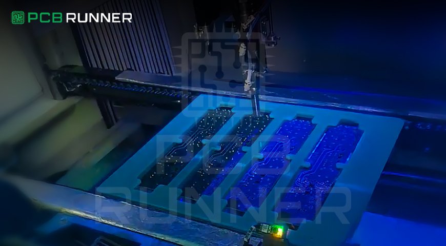
Have you ever finished your PCB design, sent it to a manufacturer, and then gotten a message saying something’s wrong with your files? If you have, you’re not alone. Many people, whether you’re a student, hobbyist, or engineer, run into trouble with Gerber files. These little files are super crucial for printed circuit board manufacturers. They tell the factory exactly how to make your board. But if there’s a mistake, your project can get delayed, cost more, or even fail.
Let’s walk through the most common Gerber file mistakes, how you can spot them, and what you should do to fix them. By the end, you’ll know how to make your PCB manufacturing process smoother and avoid those stressful emails.
What Are Gerber Files, and Why Should You Care?
Gerber files are like the blueprints for your printed circuit board. They show every detail, where the copper goes, where to drill holes, where the writing should be, and where the solder mask covers the board. If your Gerber files are wrong, your board will be wrong, too.
Printed circuit board manufacturers rely on these files to make sure your board turns out just how you want it. If you want your PCB manufacturing to go well, you need to get your Gerber files right.
Most Common Gerber File Mistakes (And How to Fix Them)
1. Missing Layers
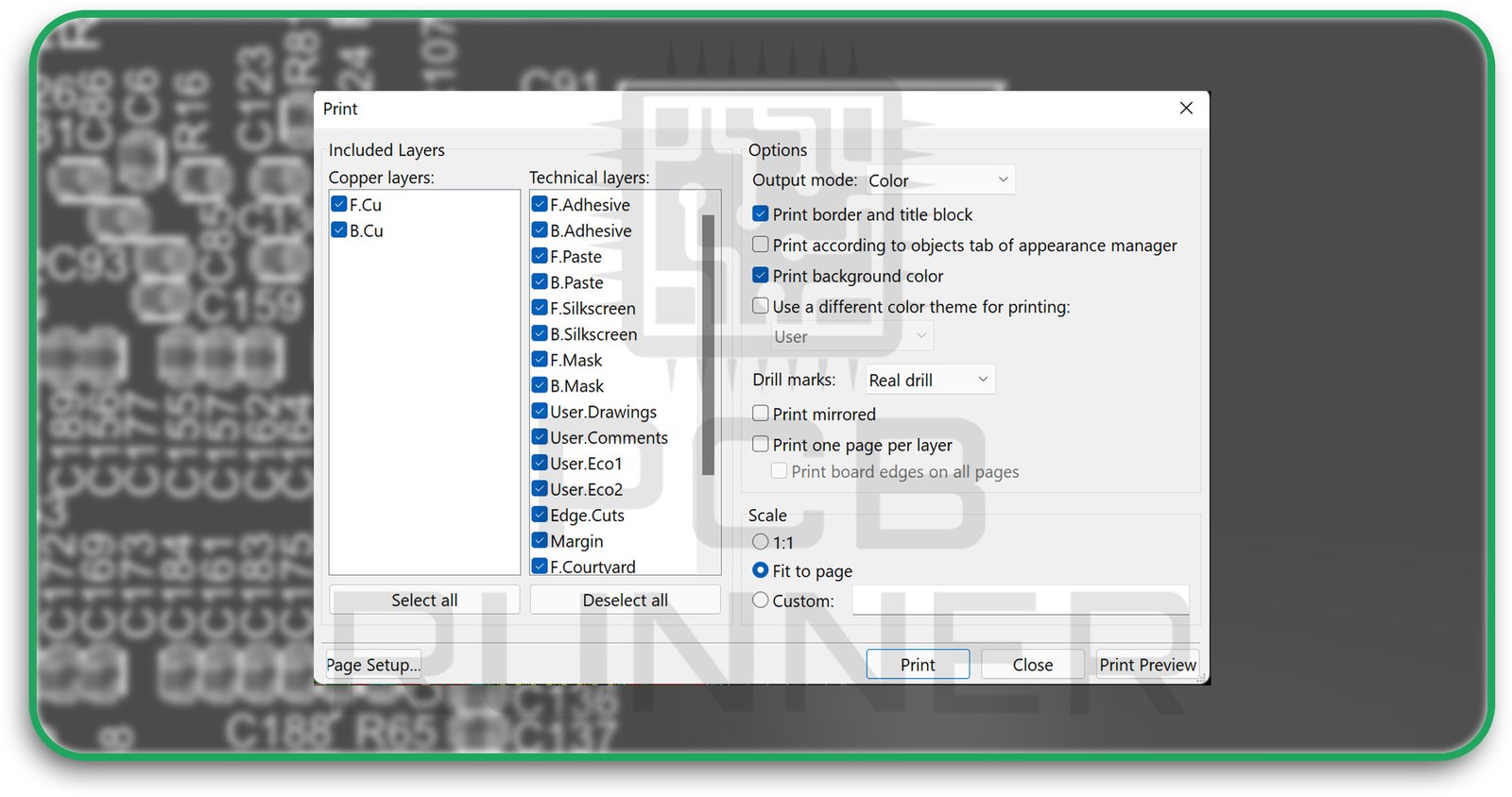
One of the most significant problems is forgetting to include all the layers. Maybe you left out the solder mask or the silkscreen. Sometimes, people even forget the outline of the board. If you leave out a layer, your board might not work or could be impossible to build.
How to fix it:
Before you send your files, check that you have all the layers. You should have copper layers (top and bottom), solder mask layers, silkscreen layers, a drill file, and a board outline. If you’re not sure, ask your printed circuit board manufacturers for a checklist.
2. Wrong Layer Names
It’s easy to mix up the names of your files. But if the names aren’t clear, the factory might not know which file is which. This can lead to mistakes or delays.
How to fix it:
Use simple, clear names for each file. For example, call the top copper layer “TopCopper” and the bottom silkscreen “BottomSilkscreen.” If you’re confused, include a text file that explains which file is which.
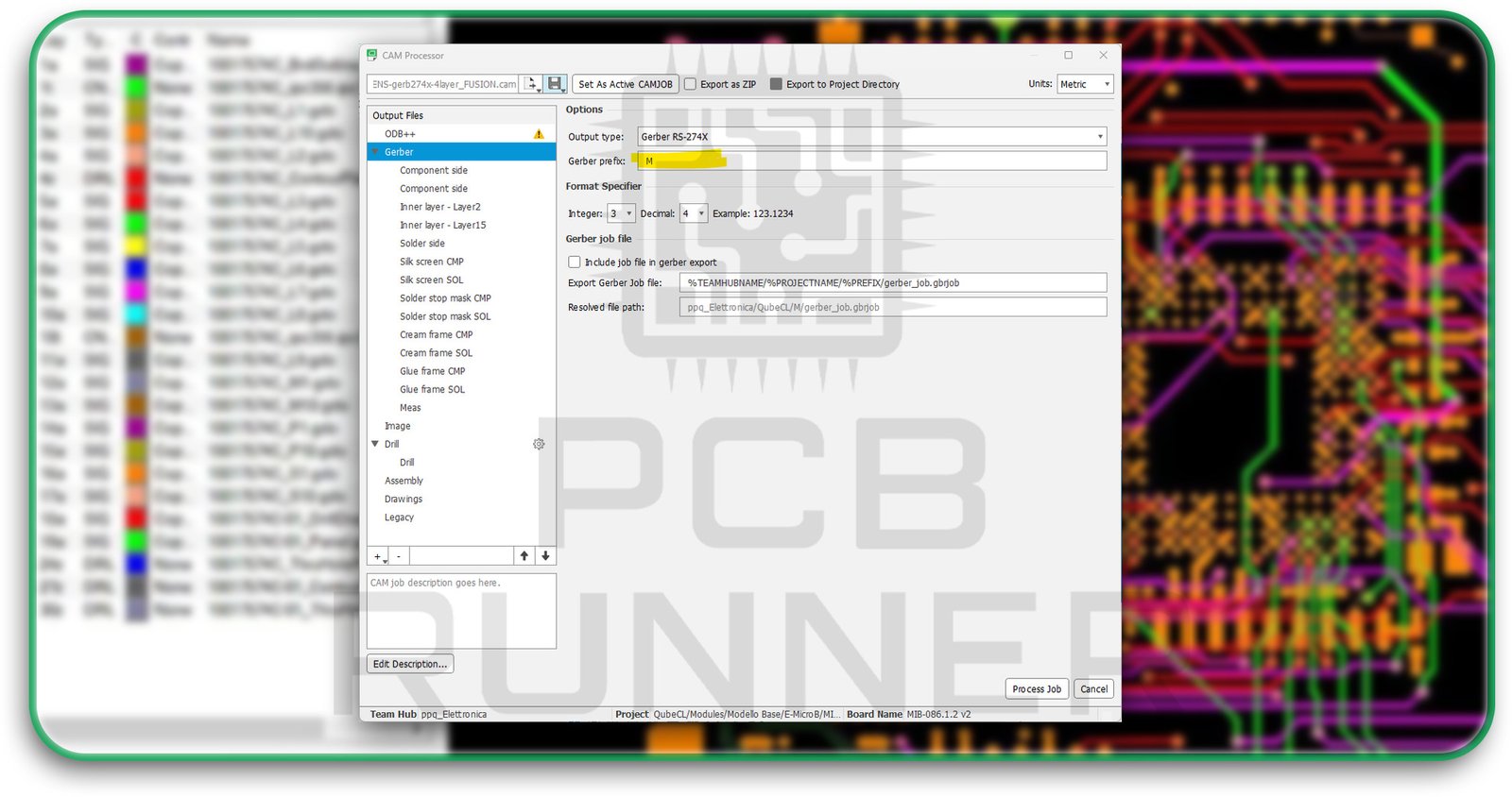
3. Outdated or Wrong File Format
Not all Gerber files are the same. Some are old formats that don’t have all the info the factory needs. If you use the wrong format, your board might not be made right.
How to fix it:
Always export your files in the RS-274X format. This is the most common and has all the details the factory needs. If you’re not sure, check with your printed circuit board manufacturers before you send your files.
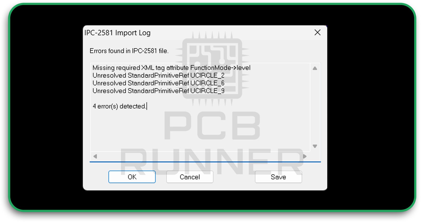
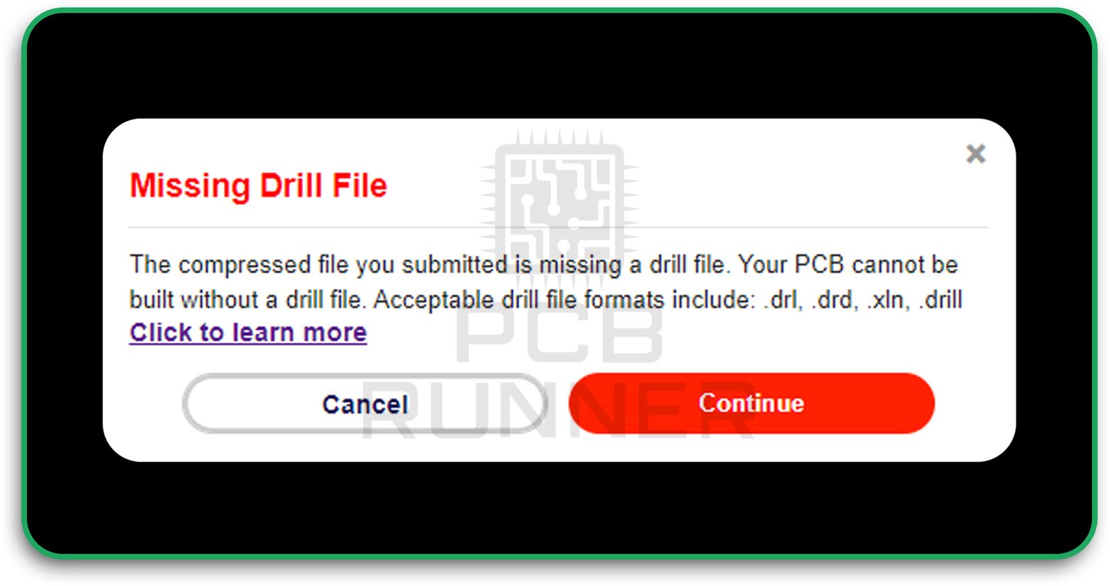
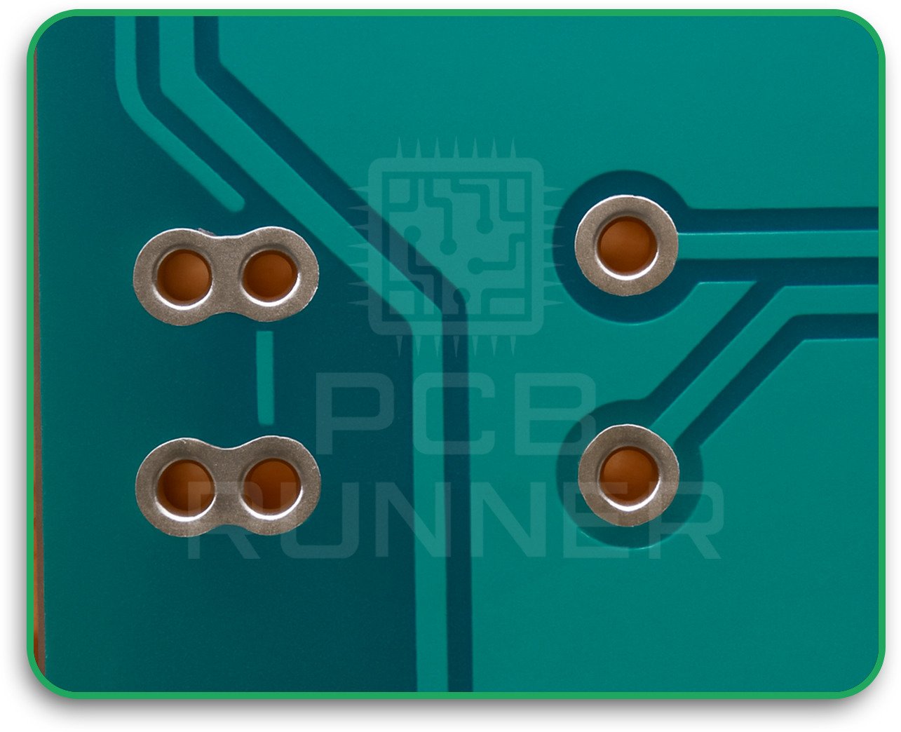
4. Drill File Problems
Drill files show where to put holes for parts and vias. If you forget the drill file or use the wrong format, your board can’t be made.
How to fix it:
Always include a drill file, usually called “.drl” or “.txt.” Double-check that the holes in your file match the holes in your design. If you view Gerber files with a Gerber viewer, you can see if the holes line up right.
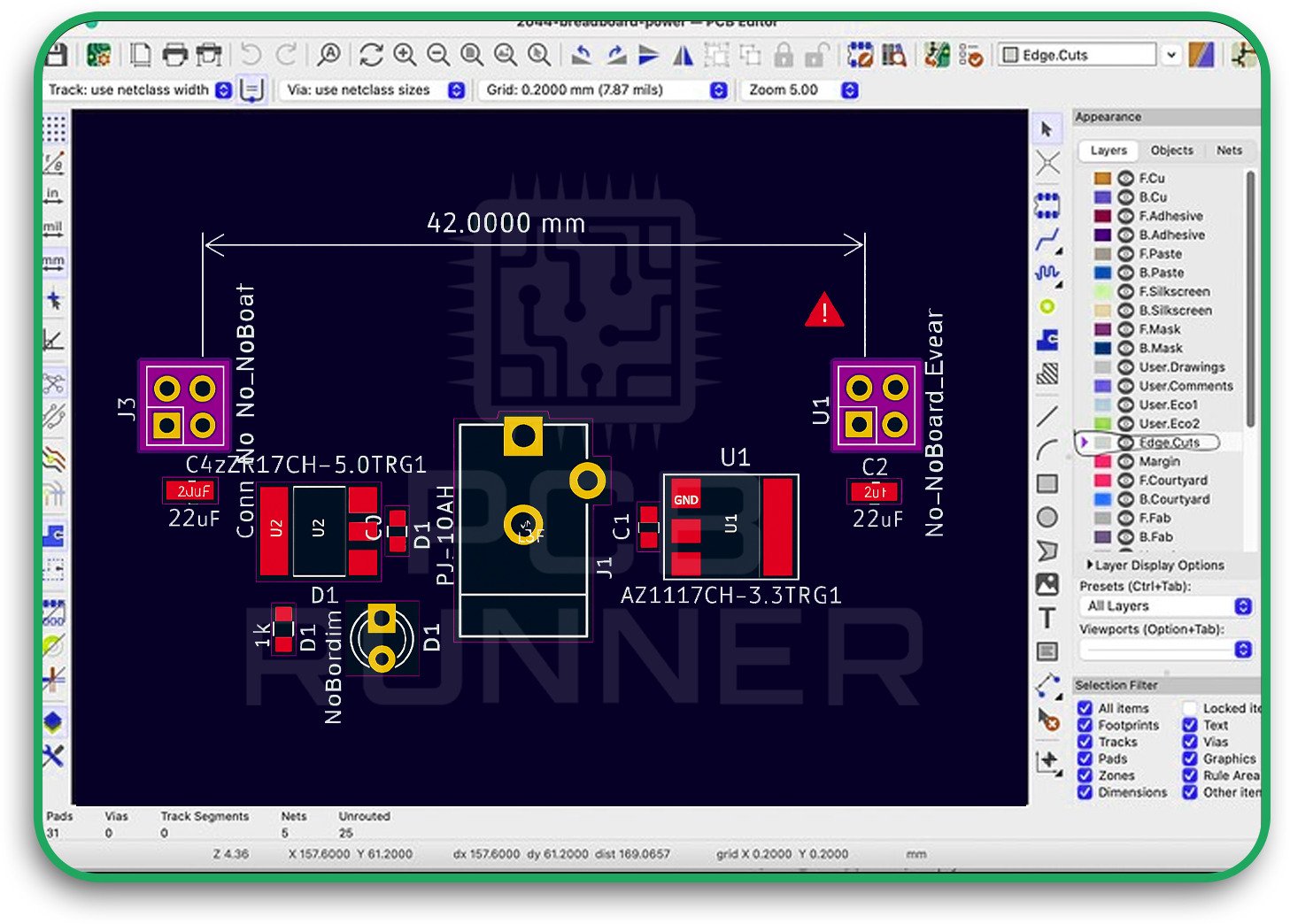
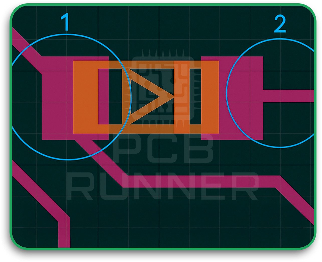
5. Misaligned Layers
Sometimes, the layers don’t line up. Maybe the solder mask doesn’t match the copper, or the silkscreen is off. This can cause shorts, open circuits, or just make your board look bad.
How to fix it:
Use a Gerber viewer to check your files before you send them. Look at all the layers together to make sure they line up. If something looks off, go back to your design and fix it.
6. Missing Board Outline
If you forget to include the outline of your board, the factory won’t know what shape or size to make it.
How to fix it:
Always include a board outline file. Name it clearly, like “BoardOutline” or “Mechanical.” This helps your printed circuit board manufacturers know exactly what you want.
7. Pads or Traces Too Small
If your pads are too tiny or your traces are too thin, the board might not work or could break easily.
How to fix it:
Check your manufacturer’s rules for the smallest pad and trace sizes. Make sure your design follows these rules before you export your Gerber files for PCB manufacture.
8. Overlapping or Duplicate Shapes
Sometimes, you might have two pads or traces in the same place by mistake. This can confuse the factory and cause problems.
How to fix it:
Clean up your design before you export. Use your design software’s error checker to find and fix duplicate or overlapping shapes.
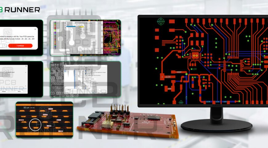
How to View Gerber Files Before Sending
Don’t just hope your files are right, check them! There are free Gerber viewers you can use online or download. When you view Gerber files, you can see exactly what your manufacturer will see. This helps you spot missing layers, misaligned parts, or other mistakes.
Tips for viewing Gerber files:
- Open all your files in the viewer.
- Look at each layer one by one.
- Check that everything lines up.
- Make sure the board outline is clear.
- Zoom in to check small details.
If you spot a problem, fix it in your design software and export the files again.
Why Printed Circuit Board Manufacturers Care About Gerber Files
Your manufacturer wants your board to turn out right. But if your files are wrong, they have to stop and ask you for new ones. This slows down the process and can cost you extra money.
Good printed circuit board manufacturers will often review your files and let you know if something’s wrong. But it’s always better to catch problems yourself first. This saves time and helps your PCB manufacturing go smoothly.
Best Practices for Sending Gerber Files
- Check every layer: Make sure nothing is missing.
- Use clear names: Don’t make your manufacturer guess.
- Include a readme file: Explain what each file is if you’re not sure.
- Ask for help: If you’re confused, ask your manufacturer for advice.
- Keep files together: Put all your files in one folder before sending.
What to Do If There’s a Problem
If your manufacturer says there’s a problem with your Gerber files for PCB, don’t panic. Here’s what you should do:
- Ask them which file or layer is wrong.
- Open your files in a Gerber viewer and look for the issue.
- Fix the problem in your design software.
- Export the new files and recheck them.
- Send the corrected files back to your manufacturer.
Real-Life Example: A Simple Mistake
Let’s say you’re making a small sensor board. You design it, export your Gerber files, and send them off. The manufacturer emails you back: “Your drill file is missing.” You check and realise you forgot to export it. You fix the mistake, send the new file, and the board is made perfectly.
This kind of thing happens all the time. By learning to view Gerber files and double-check your work, you can avoid simple mistakes and keep your project on track.
Why Getting Gerber Files Right Matters for You
If you want your PCB manufacturing to be fast, easy, and successful, you have to get your Gerber files right. It saves you time, money, and stress. Plus, your printed circuit board manufacturers will be happy to work with you again.
Action Steps for Your Next PCB Project
- Always view Gerber files before sending them.
- Use a checklist to make sure nothing is missing.
- Name your files clearly and keep them organised.
- Don’t be afraid to ask your manufacturer questions.
- Fix mistakes quickly and learn from them for next time.
Final Thoughts
Gerber files are the key to making your PCB project a success. Even small mistakes can cause significant problems, but with a bit of care and the right tools, you can avoid them. Always check your files, communicate with your printed circuit board manufacturers, and follow best practices. That way, your PCB manufacturing will go smoothly, and you’ll be proud of the boards you create.