Solder Mask Types & Colors

Exploring PCB Solder Masks: Types, Colors, and Future Trends

Introduction:

Printed circuit boards (PCBs) are coated with a polymer layer known as solder mask (sometimes called solder resist) to control solder spreading and avoid solder bridges during assembly. Additionally, it aids in shielding traces from electrical leaks and environmental deterioration. To assist PCB designers in making the most effective use of this crucial material, this page discusses solder mask types, qualities, functions, design concerns, application techniques, and faults.

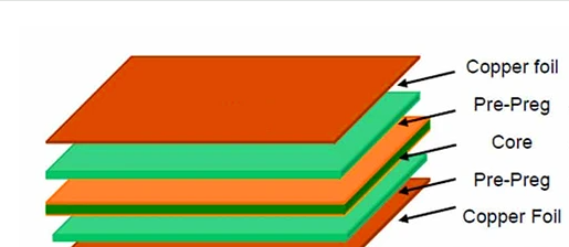
Applied permanently on the surface of finished PCBs, solder mask—also referred to as solder resist, solder stop, or solderable mask—is a thin layer of insulating material similar to lacquer. The solder mask’s primary purposes are as follows: 

  • Preventing environmental corrosion and oxidation of exposed copper 
  • Preventing the formation of solder bridges during assembly between pads that are closely spaced. 
  • Live nets that are electrically insulated to avoid shorting. 
  • Enabling the selective plating or coating of exposed portions 

Most completed circuit boards have a green solder mask covering most of the surface, leaving exposed metalized pads and traces for soldering. It adds a unique look to manufacturing boards in addition to silkscreen.

However, solder masks have uses far beyond aesthetics. Correct design and use significantly improves the manufacturability and reliability of PCBs.

Four Primary PCB Solder Mask Types  

Solder mask, sometimes referred to as solder resist, is a robust, long-lasting coating that shields printed circuit boards’ (PCBs) copper traces and their interfaces. A solder mask’s primary purpose is to stop conductive solder from bridging between various electrical components and creating short circuits. There are numerous varieties of PCB solder masks, including top- and bottom-side masks, epoxy liquid, liquid photo imageable, and dry film photo imageable.

Masks on the Top and Bottom 

The electronic engineer can see the holes in the green solder mask layer that was applied to the PCB using film, epoxy, or ink processes by using a topside solder mask. Using those marked locations, component pins can subsequently be soldered onto the board. Top traces refer to the conductive trace pattern on the top side of the circuit board, whereas bottom-side mask designates openings on the lower surface.


Liquid Epoxy 

The least expensive kind of solder mask is epoxy liquid, which is silkscreened onto the PCB layout. The thermosetting polymer epoxy has a wide range of uses. A woven mesh is used in the printing process known as “silk screening” to support stencils or patterns intended to obstruct ink.

Ink can transfer to open spaces created by the mesh. While silk is frequently employed in art, synthetic fibers are more frequently used in electronic applications. Thermal curing is the last step in the finishing process.  

Fluid Ink Capable of Photo image  

The liquid photo imageable solder mask is supplied in the form of an ink. The PCB can be coated with ink by spraying or silk screening it, exposing it to the design, and then developing it. Hot air surface leveling is one kind of procedure that is frequently employed with liquid ink formulations (HASL). It needs a spotless setting devoid of impurities and particles. Following the UV light exposure phase, developers—high-pressure water sprays—are used to remove the mask. Thermal curing and organic coating are necessary for circuit board finishing.

Photo imageable Dry Film  

Vacuum lamination is used to apply a dry film photo imageable solder mask, which is subsequently exposed and developed. Parts can be soldered to the copper pads once the pattern has been established after development. Electrochemical processing is used to layer copper onto the board inside the holes and on the trace sections. The copper circuitry is shielded with tin. After that, the exposed copper is etched and the dried film is removed. Thermal curing is another step in finishing.

Factors influencing the solder mask color selection

Visibility and contrast  

Enhancing the contrast and visibility of your PCB marks and components is a primary motivation for selecting a solder mask color. If you use a magnifying glass or a microscope, a high contrast color can assist you locate and examine the vias, silkscreen labels, and solder connections on your PCB. Although a low contrast color can conceal certain flaws or errors, it can also give the impression that your PCB is more consistent and smooth. In general, colors that are high contrast include green, blue, and red, while colors that are low contrast include black, white, and yellow.

Both branding and aesthetics  

Enhancing the aesthetics and branding of your PCB design is another justification for selecting a solder mask color. The color of your solder mask might express your brand, your organization, or the theme of your product. For instance, you may want to pick a color that is bold or distinctive to set your PCB apart from the crowd, or a color that is subdued or neutral to go in with the surroundings. It could be a good idea to coordinate the color of your solder mask with the enclosure, your logo, or other design components. But you should also think about how the color of your solder mask influences your PCB’s durability, solderability, and heat dissipation.

Guidelines and policies  

Adhering to the rules and specifications that are relevant to your PCB design is the third justification for selecting a solder mask color. Certain industries or applications, like the military, medical, or automotive sectors, could have particular demands or suggestions about the solder mask color of their printed circuit boards. For instance, some medical PCBs use white solder mask to denote cleanliness and sanitation, whereas some military PCBs use red solder mask to show excellent reliability. Before selecting the color of your solder mask, you should always make sure it complies with all applicable rules and laws. These can have an impact on the functionality, security, and caliber of your PCB.

Price and accessibility  

Taking the price and accessibility of your PCB fabrication into account is a last justification for selecting a solder mask color. Depending on market supply and demand, different solder mask colors may have varying costs and lead times. Since most PCB manufacturers utilize and supply green solder masks, it is typically the most affordable and common hue. Certain colors could need unique materials or methods, which could make them more costly or take longer to produce. Before selecting the color of your solder mask, you should always check with your PCB manufacturer as they can have different possibilities and restrictions.

Advantages of covering bare copper on a PCB with a solder mask 

Using a solder mask over bare copper on a PCB has numerous advantages.  Among its primary advantages is its potential to shield copper from oxidation. Also, it may aid in preventing solder from bridging copper lines next to one another. By creating a barrier between the copper and the environment, a solder mask can shield the metal from oxidation and other forms of deterioration.

Furthermore, a solder mask can act as a sort of barrier between the PCB’s various conducting layers. By doing this, crosstalk can be decreased, and the PCB’s overall electrical performance can be enhanced. By creating a low-impedance channel between the copper traces, this can enhance the PCB’s electrical performance.

Design Considerations for PCB Solder masks  

Solder mask is a crucial component in assuring the correct operation and dependability of the finished product, and PCB design encompasses many other important considerations. It’s important to take a number of factors into account while designing a PCB using solder mask, including material choice, thickness, tolerances, and clearance needs. We’ll talk about these design factors in this part and offer tips to help you make the best PCB design possible for a solder mask application.  

 Selection of Materials  

Solder mask materials come in a variety of forms, as was previously mentioned, and each has special qualities and functions. Think about things like electrical insulation, flexibility, chemical resistance, and thermal stability when choosing a solder mask material for your PCB design. To select the best material, consider the needs and operation environment of your PCB.  To find out which solder mask materials are suitable for your particular design, speak with your PCB maker. 

Thickness of Solder mask  

The PCB’s overall performance, including mechanical stability, electrical insulation, and thermal management, can be impacted by the solder mask layer’s thickness. You must weigh these considerations and make sure that your design complies with industry requirements in order to decide on the right thickness. For suggestions on solder mask thickness, refer to the IPC guidelines.  To find out the maximum solder mask thickness that will work for your design and production process, speak with your PCB manufacturer.

Registration and Tolerances 

For the solder mask layer to be precisely aligned with the copper traces and pads underneath, solder mask tolerances and registration are essential. To prevent solder bridging or shorts during assembly and to shield delicate components from the elements, alignment must be done correctly.
Utilize the solder mask design guidelines and tolerances that are acceptable for the capabilities of your PCB manufacturer.
Incorporate alignment features or fiducial markers into your PCB design to enable precise solder mask registration during production.

Clearances & Openings at solder mask 

The regions of the PCB where the solder mask is purposefully left off to facilitate soldering, testing, or other activities are known as solder mask clearances and apertures. For PCB assembly and functioning to be successful, these areas must be defined correctly.

Based on component pad sizes, soldering specifications, and manufacturing tolerances, design solder mask clearances.

If more space is required, add it for test points, fiducial marks, or other functional requirements.

You may maximize the performance, dependability, and manufacturability of your PCB design by giving careful thought to these solder mask design considerations.

What color of solder mask should be?
The dye that is utilized in the solder mask material determines the color of your solder mask, and the cured solder mask thickness is influenced by the chemical properties of the dye. The ability to produce thin solder mask dams (~0.1 mm) is one of the reasons green solder stop mask is so widely employed. Different colored solder mask dyes typically result in thicker solder mask dams. IPC-SM-840D defines solder resist thickness on PCBs for usage in specific industries or applications, regardless of the dye you choose to employ.

A crucial component of automated or human visual inspection is the color of the solder stop mask. The least contrast between the board and traces is produced by black solder mask, which can make automated inspection challenging. This is an additional justification for favoring green masks. During manual inspection, the color of the silkscreen you choose will also affect visual contrast and visual fatigue.


You should prepare your design to account for the sensitivity of your final application, just like you would with any other fabrication parameter or process. It’s crucial to talk to your manufacturer about your fabrication possibilities at all times. Depending on their ability, they might even be able to recommend better choices.

Which Solder Mask Is Best ? 

The physical dimensions of your board, the holes, components, and conductors, the surface layout, and the intended use of your product all play a role in selecting the right solder mask. You will need a photo imageable solder resist for the majority of contemporary printed board designs. A liquid or dry application will depend on the topography of the surface. A dry application applies a consistent layer of solder mask to the whole surface. Nonetheless, a particularly flat board surface is ideal for dry mask adhesion. For improved contact between the copper of your traces and the laminate, you’re usually better off using a liquid (LPSM) option if your surface characteristics are intricate. A liquid application’s drawback is that the thickness isn’t consistently the same. 

Additionally, you can apply various finishes to the mask layer. Discuss what your manufacturer has available and how it will impact production with them. For instance, if you are employing a solder reflow process, a matte coating helps to minimize solder balls.


Solder masks are required for PCBs produced by the solder reflow process. The quality of the reflow might be impacted by the mask’s polish.

The range of colors for Solder Masks in printed circuit boards: advantages and disadvantages 

Green

For good reason, green solder masking is currently the most widely available hue on the market. It is a suitable hue for maintenance and repairs because it provides one of the biggest visual contrasts of any accessible color between planes, traces, and empty areas.  Owing to its widespread appeal, almost all large-scale PCB manufacturing facilities can obtain it, and it is regarded as the standard hue for circuit boards globally. It is also the least costly circuit board color that is offered as a result. It has one of the thinnest coats and can hold the smallest solder mask dams to avoid solder bridging because of intensive research and development.

Red 

A visually arresting choice, red solder masking is frequently utilized in designs that highlight interior hardware. The hue is now among the most often used alternate PCB colors, but there’s a catch: it’s less visible and has less contrast than a typical green PCB. When doing maintenance on a red PCB, technicians might need to use more magnification to see problems on the board. Almost always, people choose red for its beauty rather than its usefulness. 

Blue

Though it has less contrast than circuit boards that are red, green, or yellow, blue is the second most popular hue utilized in the production of PCB boards. They are usually connected with open-source electronic projects since they are the preferred color for Arduino boards due to the way silkscreen appears on them. Furthermore, the coloration of blue solder masking makes it perfect for installation behind LCD screens.  

Black 
Compared to other colors, black solder masking is one of the priciest color options and frequently requires more time to make. It should not be used in high-heat applications because of its propensity to absorb heat. It also has very little contrast, which makes maintenance and repairs challenging. Additionally, during the production process, it has the highest failure rate.

Silkscreen looks really good on black PCBs, despite the low trace contrast on these boards. It is also the least reflective light, which makes it perfect for circuits where light is undesirable.  While black solder masking may be visually appealing to businesses such as Apple that value sophisticated design, it is seen as a challenging hue to work with from a practical standpoint. Selecting a circuit board with a black print should be done carefully. 

White  

White PCBs are the hardest to visually analyze since they have even less contrast than black PCBs. Over time, they also clearly gather dirt.  White solder masking is frequently used with LED lights, especially when they are attached to surfaces with lighter colors. When the lights are on, white offers the least noticeable color and blends in the best. Since white is one of the colors that reflects light the most, it also emits pure white light when lit.
Make sure your manufacturer is utilizing a solder with high reflectivity when choosing white PCBs for LED applications, as not all solders are created equal.

Future Trends in Solder Mask Technologies

There is a constant  exploration  for new developments in materials and methods to deliver the highest quality product possible as technology continues to advance toward tighter features and larger circuit densities. In terms of capital expenditure and collaborating with suppliers to overcome these issues related to material, process, and quality, Advanced Circuits is still in the forefront. Our investment in enhanced solder mask (SM) materials and laser direct imaging (LDI) equipment will give the best overall quality solution to fulfill current and future technological demands. Advanced Circuits Colorado will start switching to the higher performance solder mask on October 23 in order to specify the tight SM features that are frequently encountered in modern technology. This solder mask is intended for LDI.

Thermal management

More thermal management will be a top priority for solder masks in the future. This is to account for the increasing power density of contemporary electronics. Maintaining optimal performance will require improved heat dissipation qualities.

Nanotechnology

In the formulation of solder masks of the future, nanotechnology may be extremely important. Better feature resolutions and general performance enhancements might be made possible by it. Precision and miniaturization could advance as a result of this integration. 

Customization 

More customizable solder masks are probably in store for the future. This is a result of the growing popularity of flexible and wearable electronics. This will enable stretching and bending without compromising functionality. This evolution aligns with the growing demand for flexible printed circuit boards. They are employed in numerous contexts.

Conclusion 

In order to safeguard the copper traces on PCBs, solder masks are necessary. It offers defense against short circuits and oxidation. Manufacturers must to be knowledgeable about the appropriate thicknesses and methods for integrating the electronic components on PCBs. They ought to adhere to industry norms as well. Because it acts as an insulator between conductive traces, resists corrosion, and stops solder bridging, the solder mask is a crucial component of a printed circuit board. Bare copper is frequently used as traces by PCB fabrication businesses, yet it is quickly oxidized, corroded, and destroyed. When exposed to aqueous solutions, such as water, bare copper traces will oxidize as well.  Make sure a solder mask covers the copper in order to solder to bare copper effectively. If not, the copper will not be soldered to the solder. Additionally, flux should be used if you’re not soldering to bare copper and you’re not using a solder mask. 

PCB Runner offers a variety of solder masks colors including LDI & LPI methods. Do reach out to our team for custom requirements quote, you can submit your Gerber files on https://www.pcbrunner.com/free-pcb-quote/ or do reach out to our team offline at engineering@pcbrunner.com or sales@pcbrunner.com for your current or upcoming projects needs.


Type of VIAs in Rigid PCB

Exploring PCB Via Types: Choosing the Right Vias for Your Design Needs

Introduction

Vias are holes that allow conductivity to go through the board’s layers in printed circuit boards. Every hole serves as a conductive channel for the transfer of electrical signals between circuit layers. A printed circuit board has levels that vias go through. Depending on how the PCB is designed, the board may need a hole that passes through each layer from top to bottom. On the other hand, some vias go through an inner layer, while others only reach the top or bottom layer. Vias on a printed circuit board come in a variety of options. One of the most important components of a printed circuit board is the via. As a result, they bear a substantial portion of the expenses associated with the production of boards.  

Even though all of these via types have the same basic function, some PCB designs will fit one via type over another more than others. This article discusses the many via types used in printed circuit board design and how they can be used to help with electrical connections.


PCB Via Types  

On a PCB, there is a via that connects at least two layers, allowing power or signals to move between them. A copper-plated cylindrical barrel that serves as a conductive channel is present in every PCB via. In PCBs, a variety of via types are used:  

Through-hole
These  vias can connect to any layer and are available throughout the PCB stackup. Every layer of these PCB vias will feature a pad where a connection to a trace is made.  

Blind vias
These end at a landing pad and extend from an outside layer to an interior layer. Signals can then pass via an internal layer by connecting the pad to another trace.

Buried vias

These  do not reach the surface layers; instead, they extend between two interior layers. Like regular vias, buried vias can connect on any layer between their starting and terminating layers.  

Microvias
They are basically miniature blind or buried vias that span one layer at most, or two layers at most in cases of extremely thin dielectric (the latter being referred to as a skip via or skipped microvia).
stacked microvias.
Vertical stacks of blind and buried microvias, or stacks of several buried microvias, spanning multiple levels are known as stacked microvias.

Via -in-Pad
Using vias on ball grid array (BGA) pads—also referred to as via-in-pads—is one of the more widely used printed circuit board designs of today. The vias of the via-in-pad design are positioned on the PCB’s BGA pads. Because the design allows manufacturers to reduce the amount of space needed for vias, it has gained popularity. Because of this, via-in-pad enables producers to create printed circuit boards that are thinner and require less room for signal routing. For today’s small electronic and computing devices, which manufacturers have made to fit inside pockets and occasionally around wrists, via-in-pad technology is ideal.


When to Use Each Type of Via: Matching Application to Functionality

Through-hole:
This is the type of via that is used most often in a circuit board. The holes are drilled all the way through the board with a mechanical drill bit and can get down to 6 mils in size.

Buried via:
This via only connects internal layers of the board and is useful for PCBs with very dense routing. Blind via: This via starts on either the top or bottom of the board but doesn’t go all the way through it. 

Microvia:
For hole sizes smaller than 6 mils, a laser-drilled microvia is used. These vias connect only two adjacent layers of the board and can be on the surface or buried within the board layer stack up. Microvias are extremely versatile and can be stacked together, or on top of a buried via, but have a higher fabrication cost associated with them.

Via-in-pad (VIP):
These vias can either be standard thru-hole vias or microvias, but their position in a surface mount pad makes them unique. If a standard mechanical drill is used, the via will require extra fabrication steps to prevent solder on the pad from flowing down through the hole. Microvias on the other hand don’t have this problem, but they can be more difficult to fabricate due to the tighter trace and space tolerances in a high-density design.
A path that sends a signal from a source to a receiver is called a via. Effects of inductance on via design and low capacitance on signal integrity have been demonstrated. It will be demonstrated that this return path may be regulated with careful via environment design, allowing vias to be sorted out according to cable specifications within specific frequency ranges.
This indicates that the via stubs effect is addressed, as are ways to lessen it by moving undesired resources outside of the area of interest. This indicates that the via impedance can be adjusted to meet a certain goal in order to reduce reflections.

How to Choose Via’s for a PCB: 

Taking Design into Account
Assess the requirements of your PCBA project first. Evaluate factors including signal quality, heat control, power distribution, and required space. Controlled impedance vias may be required for high-speed signal traces in order to preserve signal integrity, and suitable ground and power via arrangement is essential for the best possible power distribution and heat dissipation.  

Via Size:
A device’s heat dissipation efficiency and current carrying capacity are determined by its size. Better heat dissipation and less resistance are provided by a bigger via. A densely packed PCB is better served by a smaller via. The precise design specifications determine how to strike a balance between utility and size.

Plating:
To guarantee electrical conductivity, vias are frequently plated with copper. Plating influences dependability and performance. To improve corrosion resistance, pick between through-hole copper plating and other methods like ENIG. 

Aspect Ratio:
The ratio of diameter to via depth is known as the aspect ratio, and it is important. Drilling difficulties, uneven plating, and decreased dependability might result from a high aspect ratio. When choosing the aspect ratio, consider the production capacity of the PCB manufacturer of your choice.  

Via and Layer Count:
Selection is influenced by the PCB board’s layer count. Blind and buried vias are frequently used in multilayer boards to maximize signal quality and space utilization. But producing these vias is difficult and can get expensive.

Testing and Simulation:
Analyze the effects of various vias on overall functionality, signal quality, and thermal performance by using simulation tools. Before any manufacturing happens, problems are found and the design is optimized through virtual testing.

Thermal Considerations and Heat Dissipation with VIAs

 PCB Using channels (through-holes) that pierce through the PCB, heat dissipation holes, also known as PCB thermal vias, are a technique used to dissipate heat to the backside of a PCB. They are positioned as close to or directly beneath the heat-producing element as feasible.  

By employing the PCB as a heat sink, heat dissipation holes help surface-mounted components dissipate heat more effectively. They entail drilling through holes in the PCB structurally.  Connecting the copper foil on both sides of the PCB increases the surface and volume accessible for heat dissipation, which lowers thermal resistance in single-layer and double-sided PCBs.  

The similar goal can be accomplished for multi-layer PCBs by joining the planes between layers or restraining connections to particular layers. 

Thermal Via Design  

In multi-layer boards, vias offer low heat resistance conduction channels between layers:  


Quantity
Increased via number minimizes lateral spreading before heat enters a via by reducing conduction channel lengths in the in-plane direction. But costs go up with additional vias.  

Arrangement Scheme
In comparison to peripheral distribution, gridded arrays provide superior heat dispersal from hot regions. It’s also possible to see mixed patterns.  

Density and Size
Although they take up more routing area, wider via diameters and higher via densities enhance vertical heat conduction. Laser micro-vias contribute to higher density.  

Depth
Compared to partial depth vias, full depth vias that span the entire board thickness transport heat to inner layers more effectively.

Barrel Plating Depth
Via barrels with thicker plating have less conduction loss via the via. A higher current rating is also permitted.

Size of Anti-pad
Better heat dispersal into plane layers is achieved with larger anti-pads or clearing spaces surrounding vias. However, it also shrinks the signal layers’ routing space.  

Pads for Thermal Relief
Heat from plated through-hole vias is kept out of the solder mask by exposed thermal pads. Temperatures are lowered by the enhanced heat transmission. 

Stuffing
Heat is transferred to interior layers more quickly in filled vias with conductive inserts than in hollow vias that solely rely on barrel plating.

Manufacturing Constraints and Cost Implications

Production Constraints:
It is important to consider the capabilities and constraints of the production process. Requirements for things like annular ring width, aspect ratio, minimum drill size, and pad size should match the capabilities of PCB production and assembly procedures. Respecting these limitations guarantees manufacturability and keeps possible production-related problems at bay.

Cost and Reliability:
Aspects of cost and reliability should be taken into account when optimizing the route design. While too many vias could raise production costs, improper via location or size could affect the PCB’s dependability and functionality. Achieving a dependable and affordable design requires striking a balance between these variables.

Advanced Via  Frameworks and Methodologies  

With recent developments in via fabrication, PCBs can be made denser and more complicated, enabling increased capabilities. Here are some cutting-edge technologies and via types: 

Back drilled Vias:
The stub portion of the via is removed by mechanically drilling off the via barrel after it has extended through the pad on the outer layers. This lowers stub resonance for high-speed signals considerably.  

Filled & Capped Vias:
Compared to just plated vias, completely filling a via’s hole reduces the possibility of contamination and increases heat transfer. Capped vias have protective epoxy covering only the end holes.

Tented Vias:
To completely isolate tented vias and keep solder and debris out of vias not used for component terminals, a layer of solder mask coating is applied.  

Via in Pad (VIP):
By positioning drill pads over function pad centers, VIP enables vias to be implanted straight into footprints, preventing routing channels from being blocked.  

Microvias Assisted by Lasers:
Lasers create tiny holes that are impossible to drill with mechanical tools, allowing for direct copper plating without the need for seeding.


PCB Vias Design Guidelines for Buried, Blind, and Through-Hole Vias

Every one of the aforementioned PCB kinds has unique design guidelines. The same is covered in this section.

Hole-through PCB Vias 

  • Every layer of the circuit board needs to have a drill pad for through-hole PCB vias. While it should be small, the drill pad should be big enough for the drill being used. 
  • Additionally, in order to prevent short circuits between adjacent holes, the through -hole via requires a conventional anti-pad on the board’s plane layers. 
  • Choosing the right via size is a crucial design guideline for through-hole PCB vias. 
  • The aspect ratio of the drilled hole in relation to the thickness of the board should be considered while selecting the via sizes.

The residual or unused via barrel in the multi-layer circuit board may function as an antenna if a through-hole via can connect high-speed signals between the first two layers. But this could lead to problems with signal integrity. OEMs use back drilling to get around this issue. Nevertheless, the overall cost of fabrication goes up with this procedure. To increase board performance, using blind and buried or micro vias is the ideal approach.
If necessary, through-hole vias can be covered or filled. The PCB designer gives the fabricator precise instructions for this.


PCBs buried via 

  • Buried vias, as previously mentioned, link the circuit boards’ inside layers, which are not in contact with the exterior layers. For a single connection, the hole needs to be defined as a distinct drill file.
  • Buried vias, as previously mentioned, link the circuit boards’ inside layers, which are not in contact with the exterior layers.  
  • For a single connection, the hole needs to be defined as a distinct drill file. 
  • Aspect ratios of at least 1:12 are required.  
  • The maximum distance and overall depth between the corresponding outer layers and inner layers are determined by the small hole.  
  • Mostly helpful for PCBs with thick routing are buried vias.


Blind PCB Vias 

  • Since blind vias are mechanically bored, their drill size restrictions are comparable to those of through-hole drilling. Through in-the-layer stack-up, they permit additional routing channels above or below. Blind vias have a benefit over through-holes because of this capability.  
  • Similar to buried, every hole in a blind route needs to be identified as a distinct drill line.  
  • Aspect ratios ought to be at least 1:1.  
  • The layers of the circuit board are drilled and plated before being fused together in this sort of via, which is constructed sequentially. PCB designers should therefore use them with caution and only when necessary.


How should a micro via for an advanced HDI PCB be designed? 


Hole Size:
Modify every component of a PCB that has been traditionally intended for microvia design. excessively large holes, or those that will produce a small PCB that is not functional or not ideal.  

Copper Thickness:
The circuit is connected throughout thanks to patterned plating. Conversely, wire bond plating might be chemical or electrical. Produce robust and stiff FR4 laminates with thin micro double-sided or single circuits for micro via design in order to ensure reliability. 

Security Marking:
For accurate PCB identification, very tiny individual barcodes can be imaged onto the solder mask.

Future of PCB vias 

The PCB industry’s automated assembly technology is a future trend.

SMT Vias 

With well-known PCBA manufacturers like JCLPCB and PCB Way embracing this technology, digital intelligence has clearly emerged as a prominent trend in the PCB market. A significant amount of PCBA boards are becoming more and more necessary as market demands change. As a result, Surface Mount Technology has taken the lead and now holds around 70% of the market. 

In order to finish PCB assembly, component leads are manually placed into drilled holes on the PCB and soldered to the copper traces on the other side of the board using the conventional Through-Hole Technology. By placing components directly on the PCB surface, the SMT method, on the other hand, avoids the requirement for drilling holes thanks to automated equipment. This comprises a variety of parts, including integrated circuits, resistors, and capacitors. 

Build up technology for vias 

A common method for creating HDI advanced PCBs is the build-up technique. The inner and outer layers of a multilayer PCB are typically made independently and then pressed together. Additionally, we start with the creation of the inner layers and work our way outward, adding layers on both sides. Laser lasers are typically used to drill blind or buried vias in order to expedite the production process. Furthermore, the build-up technique can result in circuits with finer trace and spacing up to 2 microns. However, plating micro-vias still requires more sophisticated equipment, making it more expensive and challenging.

Via Filling 

We may have problems with air bubbles remaining in the laser-drilled blind or buried vias, which impacts the thermal shock resilience of advanced PCBs. The traditional techniques involve using a resin or unique resist to fill the blind or hidden vias. These techniques are not very efficient, though, and they are challenging. Via filling is introduced to fill buried or blind vias by electroplating, which significantly boosts reliability, in order to improve processing. More sophisticated machinery, specialized plating solutions, and the necessary copper weight are required to achieve effective filling, which nevertheless entails difficulty and high expense. PS Electronics is happy to be involved in the development of other cutting-edge PCB technologies, such as Lo PCB, Rigid-flex PCB, and High-frequency PCB. 

Conclusion 

Vias are required to manufacture multilayer PCBs, which are the way of the future for PCB manufacturing. These PCBs are required to produce the highly functional and compact devices that are the mainstay of modern electronics.

The movement of heat and electrical current between the various layers of a board is facilitated by vias. These vias differ in size and type as well. The kind and dimensions of vias to be used depend on the needs of a circuit board. Vias also improve the signal integrity of circuit boards. Throughout the board, annular rings and multilayer lamination are crucial. Additionally, when creating vias, copper pad and surface components are essential. In PCBs, many vias and signal lines are frequently employed. The outer layers hold significance as well.

PCB Runner handles all type of Via’s categories including blind, buried, stacked & staggered via’s. Do submit your gerber files on https://www.pcbrunner.com/free-pcb-quote/ or do reach out to our team offline at engineering@pcbrunner.com or sales@pcbrunner.com for your current or upcoming projects needs.

pcb prepregs

Core/Prepreg Thickness

Understanding PCB Cores and Prepregs: Properties, Selection, and Future Trends

Introduction

In essence, PCB cores are one or more prepreg laminates that have been heated, pressed, hardened, and cured. Copper foil is applied on both sides of the core.  The PCB’s isolating substance is called Prepreg Core. Prepreg serves as both a multipurpose inner conduction medium for PCBs and a binding agent. A resin is infused into prepreg material; the resin is not cured but toughened. Consider the prepreg to be the binding agent that keeps the main components together. A prepreg laminate will start to bond to the neighboring layers when two cores are layered on each side then heated and compressed. The crosslinking process of the hardened resin gradually cures it, bringing its final material qualities closer to those of the core layers.

There is a glass weaving in the resin substance. Using a loom, the weave can be made tight (7628 prepreg, for example) or loose (1080 prepreg, for example) during production. The final product’s electromagnetic properties (dispersion, losses, and any fiber weave effects observed by signals in the board) are determined by the gaps and homogeneity of the glass weave.

Prepreg Thickness

Prepreg in PCBs 

Insulation is the primary function of prepreg in PCB construction. It is a layer of building material that sits between the inner core and the copper surface of a board. Its function is to operate as a dielectric substance between these layers to stop current flow. It is frequently referred to as a binding substance and is utilized to help strengthen a board because of the way it is linked between these layers. A prepreg layer can be modified in a variety of ways by the client, such as adding chemicals and catalysts to make it more conductive or to boost insulation.

Since prepreg is made of fiberglass cloth coated in a resin reserve, it is simple to attach to core material. Glass strands are knitted together to create a glass tissue, which is then given time to partially dry. It acquires an adhesive characteristic when it is pasted over the core substance. Designers monitor the material’s volume friction prior to adhesion because it will ultimately decide the prepreg layer’s final characteristics. This is the point at which manufacturers modify it to satisfy client specifications. Thankfully, this versatility implies that a wide range of prepreg materials can be found to satisfy practically any requirement. It’s a terrific extra skill because of its easy application and mastery. Additionally, the weight of a board can be decreased by adding a prepreg layer, which makes board design downsizing easier.  

PCB core 

Both single-sided and double-sided PCBs are built using a core. The base upon which we build the entire board is known as the core material. It’s a solid plate that you may coat with copper (and Prepreg for insulation) on one or both sides.  An FR-4 (Flame Retardant) mixture of components, including copper traces and titanium epoxy laminates, make up a core. It is woven with fiberglass fabric to produce a solid surface that resists fire. After that, copper is applied on both sides of it to create the PCB’s foundational material. By itself, it produces a stable, pliable surface that can be used to assemble parts. Its strength significantly rises with a prepreg layer without adding a lot of extra weight. To build multilayer PCBs, the majority of electronic manufacturing services mix the two.

Properties of PCB Prepregs

Qualitative characteristics in prepregs for superior PCBs:  

Dielectric Constant: Low dissipation factor and stable dielectric constant are necessary for high frequency performance. 3.5–5 values are normal for prepregs made of glass fiber and epoxy.  

Low Z-axis shrinkage and expansion during temperature cycling prevents via failures and is a sign of dimensional stability. X-Y shrinking often less than 0.5%.  

Bond Strength: Excellent resistance to delamination and strong adherence to prepreg layers and copper foils. Strength of bond > 2.5 N/mm.  

Decomposition Temperature: A high Td above 300°C minimizes charring problems and indicates stable thermal performance.

Moisture Absorption: Low affinity for moisture guards against vapor pressure-related reliability problems and electrical leakage. Uptake standard <0.5%.  

Flow and Filler: Sufficient resin flow to cover defects, but not too much to prevent wire shorts. Filler loading ranges from 15% to 40%.  

High level of resistance to burning, igniting, and producing smoke is known as flame retardancy. Material certified UL 94 V-0.

Properties of PCB core

1) Thermal characteristics  

The amount of heat that a substrate can tolerate is determined by its thermal property. The whole PCB’s heat tolerance level is determined by the substrate’s heat tolerance levels. Furthermore, the PCB’s heat conduction levels are determined by its thermal characteristics. 

Glass Transition Temperature (Tg): 

Temperatures over a specific threshold cause a PCB substrate to soften. After being taken out of the heat, the substrate hardens back to its original state. The glass transition temperature (Tg), expressed in degrees Celsius, is the range at which a substrate can undergo this transformation. 

Decomposition Temperature (Td): 

A PCB substrate will break down if it is subjected to temperatures over a particular point. The PCB loses five percent or more of its total mass throughout this procedure. Decomposition temperature (Td), expressed in degrees Celsius, is the range of temperatures where this process takes place.

Coefficient of Thermal Expansion (CTE): 

The CTE of a PCB is the measure of its rate of expansion. Parts per million (ppm) is a measure of a substrate’s CTE, which increases when the material is exposed to temperatures over its Tg. Generally speaking, a substrate will have a higher CTE than a copper layer.

Thermal Conductivity (k): 

A PCB’s capacity to conduct heat is measured in watts per square inch. The PCB’s capacity to transfer heat is closely correlated with a material’s thermal conductivity. The amount of heat transfer will be low if the k-level is low, and vice versa. At Kelvin (K), thermal conductivity rates are expressed in watts per meter (W/M).Many dielectric materials have a thermal conductivity range of 0.3 to 6 W/mk. In contrast, the k-level of copper is 386 W/M-ºC. As a result, in a PCB, the copper layer transfers heat more quickly than the dielectric.

pcb prepregs

2) Electrical Characteristics  

The electrical conduction in the PCB is one of the substrate’s electrical properties. Signal propagation speed between components is determined by electrical characteristics. The electrical characteristics of a PCB substrate impact and define several aspects such as bandwidth and signal transmission speed.

Dielectric Constant or Relative Permittivity (Er or Dk): 

Impedance and signal integrity are two of the key elements that affect a dielectric constant’s electrical performance. A PCB material’s relative permittivity (Dk), also known as its dielectric constant (Er), typically ranges from 3.5 to 5.5. 

Tan δ or Df, the Dielectric Loss Tangent or Dissipation Factor: 

 indicates how much less power a material loses when its loss tangent is small. Materials used in printed circuit boards typically have a dielectric loss tangent (Tan δ) between 0.02 and 0.001.Volume Resistivity (ρ): A dielectric material’s volume resistance (ρ) is its resistance to insulation or electricity. High resistance PCB material will not likely facilitate electric charges. Ohm-meters (Ω-m) and ohm-centimeters (Ω-cm) are measures used to determine how resistive a certain dielectric is. A printed circuit board’s material needs to have high resistivity, ideally between 103 and 1010 Megaohm-centimeters, just like all other dielectric insulators do.

Surface Resistivity (ρS): Surface resistivity (ρS) is the resistance of a dielectric medium to insulation and electricity. Similar to the ρ level of a material, the ρS needs to be high, ideally between 103 and 109 cMegaohms per square. Just like ρ, moisture and severe temperatures can affect a material’s ρS level.  

Electrical Potency:

 Electrical strength, expressed in Volts/mil, is a dielectric material’s capacity to withstand an electrical breakdown over a printed circuit board’s Z direction. The electrical strength of the majority of PCB materials ranges from 800 V/mil to 1500 V/mil.

Chemical characteristics 

Chemical attributes include any aspect of a PCB substrate’s chemical makeup. This describes the components of the PCB substrate’s chemical makeup. The toughness of a PCB is determined by its chemical makeup.

Flammability Specs (UL94):
The Standard for Safety of Flammability of Plastic Materials for Parts in Devices and Appliances (UL94) ranks the flame-retardant qualities of plastics, sometimes referred to as plastics flammability, from highest to lowest. UL94’s PCB material standards stipulate that specimens must not burn with blazing combustion for more than 10 seconds. A collection of five specimens cannot burn together with blazing combustion for more than 50 seconds.

Moisture Absorption:
The ability of a dielectric material to tolerate being submerged in liquid is known as moisture absorption. The moisture absorption values of most PCB materials range from 0.01 percent to 0.20 percent.

Methylene Chloride Resistance:
The resistance of a dielectric to methylene chloride absorption is the most direct indicator of a PCB material’s chemical resistance, and it is known as methylene chloride resistance (MCR). The MCR range for dielectrics is typically 0.01 percent to 0.20 percent.

Mechanical characteristics 

A PCB’s mechanical characteristics, such as its substrate’s hardness, plasticity, density, and resistance to corrosion, are used to determine its characteristics. Depending on your PCB’s intended use, the mechanical characteristics play a significant role in selecting the ideal PCB substrate. 

Peel Power:
Peel strength is the ability of the copper and dielectric layers on a printed circuit board to bind. Peel strength is measured on one-ounce-thick copper traces in three different settings during the PCB manufacturing process: after thermal stress, at high temperatures, and after chemical exposure. 

Flexural Strength:
Measured in kilograms per square meter or pounds per square inch, flexural strength refers to a dielectric material’s capacity to withstand physical stress without breaking. A printed circuit board’s flexural strength is evaluated by applying force at the middle, with only the ends supported.

Density:
The density of a dielectric material is expressed in terms of grams per cubic centimeter, or g/cc. Alternatively, pounds per cubic inch (lb/in^3) can be used to express PCB density.  

Time to Delamination:
This phrase refers to the length of a dielectric material’s resistance to influences that cause delamination. It establishes the amount of time that a PCB’s layers will remain separated from one another when exposed to temperatures that above a specific threshold. Any PCB material, including fiberglass and laminate, is susceptible to delamination from heat shock or moisture.

Selecting the Right Thickness for Your Project Requirements

Choices for PCB Thickness: 

The total thickness of your PCB is determined by the number of layers on it. While certain applications call for a thinner PCB, others require a thicker one. Thus, there are wide variations in the thickness norms. The combined thickness of the prepreg and core typically ranges from 0.008 to 0.240 inches.  

Conventional PCB Thickness: 

Single-sided, double-sided, and multilayered PCBs are all possible. The standard thickness, 1.57 mm or 0.063 inches, is a holdover from earlier standards. This is a result of the plywood industry’s use of 0.063-inch plywood sheets as substrates for electrical equipment. However, the thickness range that you can choose from now is 0.008-0.240 inches. The advancement of multi-layer PCBs is to blame for this.

Selecting the PCB Thickness: 

Keep in mind that a thicker board has a lower chance of breaking than a thin one when selecting thickness. It is preferable to stay with a thick board unless the application specifies otherwise. When selecting the PCB thickness, the following considerations should be made. 

  1. Weight: Because a thinner board is more brittle, it will break more easily. Therefore, unless the applications call for a thin board, thicker boards are preferred.  
  2. Flexibility: While thinner boards are more pliable than larger ones, they are also more prone to breaking. Thick boards weigh more and have less flexibility.  
  3. Space Requirement: A thicker board is preferable if your device has enough room for a larger PCB; on the other hand, a smaller board will be needed if your device is smaller.  
  4. Components and connections: A specific thickness will also be needed depending on the kind of connectors and components you choose.  
  5. Impedance: The board’s thickness and impedance must be matched. This is so because the dielectric, which aids in impedance control, is essentially the same thickness as the board.

Electrical Conductivity 

The electrical conductivity and signal quality that flow through the PCB are also impacted by its thickness. Because they have less resistance, thicker PCBs can handle higher current levels without overheating or making noise. Conversely, thinner PCBs can produce more noise and distortion, have more resistance, and worsen signal quality, all of which can impair the circuit’s performance.

PCB Thermal Design Factors

To get you started with addressing the thermal considerations in your design, consider the following design guidelines.
As a general rule of thumb, your board should have an area of 15.3 cm², or 2.4 in², each watt dissipated for a 40°C rise in board temperature in order to dissipate 1 watt of power. This demand can be reduced in half (7.7 cm² or 1.2 in² per watt) if the board is exposed to airflow. These numbers presuppose that the board is positioned to allow free airflow around both sides and that the component is thermally linked to a copper plane that reaches to the board’s corners. An external heat sink might be necessary if these power density specifications are too restrictive for your design. Additionally, a temperature rise of 40°C is a decent place to start when it comes to circuit board temperature control.
a. It is recommended practice to arrange power components on a board so that they heat your PCB uniformly whenever there are several power components present. Significant temperature variations along your PCB design prevent your PCB from efficiently transferring thermal energy away from the installed power components. After a design revision is finished, thermal imaging, if provided to the designer, can enable the empirical inspection of your component location.

b. Your PCB will transfer heat energy to the linked copper plane more effectively the more vias you can put beneath your component. Increase the number of vias in contact with your package’s power pads (the sizable, thermally conductive pads of the component) by using array vias.

c. You will need to utilize larger copper weights in designs that dissipate more energy. For power designs, it is advised to start with one ounce of copper.

d. Tracks that run perpendicular to the thermal path away from the power component must not obstruct the pour of copper when using it to dissipate thermal energy away from a component.

e. It should be noted that if a heat sink is required to maintain the system’s temperature within tolerance, its effectiveness will usually be significantly increased if it is positioned so that it is thermally connected to the component’s case.

Usually, this entails mounting the heat sink on the board’s other side from a surface-mounted component. Although it could be tempting to put a heat sink right on top of the component, the plastic case’s thermal resistance will make the heat sink useless. As previously mentioned, packages specifically intended to have heat sinks connected to their “tops” are an exception to this rule.

Mechanical Strength  

Impact resistance, flexural strength, and tensile strength are important mechanical characteristics to consider. The material’s resistance to bending is measured by flexural strength, whereas its tensile strength indicates how well it can tolerate stretching pressures. Conversely, impact resistance assesses the material’s capacity to tolerate shocks or abrupt impacts. The resistance of your board to breaking or deforming under bending load. IPC-6013C stipulates that stiff, flex, and rigid-flex standards must be followed.

Dimensions: Density (g/cm3): the mass per volume of a dielectric

 Time to Delamination: the length of time a PCB’s layers will stay bonded when exposed to temperature changes or moisture; Peel Strength: the resilience of copper layers and dielectrics under thermal and chemical stress.

FACTORS INFLUENCING PCB PRICES 

The kind of material, the size of the board, and the number of layers are the three variables that have the biggest effects on the breakdown of PCB manufacturing costs. The finish and the size of the holes, including these eight, are further considerations that can affect the cost.  

 Selection of Materials 

The cost of a circuit board is always going to depend on the materials that go into it. The FR4 material used to laminate standard PCBs is insufficient for boards intended for high-intensity applications, such those used in the petroleum and aerospace sectors. The selection of materials used affects a PCB’s cost. 

Different materials make up PCBs, and the choice of these materials has an impact on the final cost. The quantity of material used to produce PCBs is also greatly influenced by the size of the circuit board. Costs can be decreased by maximizing the reduction of material utilization. Additionally, when choosing materials, other aspects like mechanical qualities, thermal performance, temperature dependability, and signal performance should be considered.

PCB Dimensions 

 Modifying a PCB’s dimensions and form has a big impact on production costs. The final product will cost more since enlarging the PCB will take more material and time.  As the PCB’s surface area increases, so does its cost, thus you can figure out how much more it will cost for sizes that are larger than the typical ones. It’s crucial to remember that a PCB’s price is determined by both its overall size and the amount of space that each component takes up.

Quantity and Scale: 

The cost per unit of PCBs is directly influenced by the quantity produced. Economies of scale are frequently realized in large-scale production and batch manufacturing, which lowers the total cost per PCB. Prototyping and smaller production runs, however, are typically more expensive because of the lower production volumes.

Supply Chain and Procurement: 

The cost of producing PCBs can be affected by the selection of suppliers, the sourcing of materials, and procurement tactics. Saving money can be achieved by maintaining material quality, choosing reputable suppliers with competitive prices, and streamlining logistics and transportation. Additionally, there can be financial benefits to investigating outsourcing choices and forging solid alliances.

Technological Developments and Market Trends: 

Both might have an impact on the price of producing printed circuit boards. The efficiency and cost of production can be affected by the introduction of new materials, industrial processes, and automation technologies. In order to stay competitive, manufacturers may also be compelled to streamline operations and cut expenses due to price constraints and market rivalry.

Important Technologies for High Density PCBs  Several sophisticated processes for PCB fabrication are necessary to produce the high-density boards that are required today:  

Drilling Using Lasers  

The five mil and smaller via diameters exhibited in HDI are not achievable with mechanical drilling. These tiny vias are precisely and tightly drilled using UV lasers. Along with producing cleaner walls, laser technology also prevents smears and epoxy blockage caused by microscopic particles.  

Minimal Dielectrics  

For high speed HDI boards, standard glass fabric substrates are excessively thick and lossy. The popular low-loss thermoset laminates with dielectric thicknesses as low as 25 μm include Teijin’s Nexus and Panasonic’s Megtron 6. They avoid problems with signal integrity and permit tighter lines or spaces.

Direct  Imaging  

Rather than using a mechanical print-and-etch process, photolithographic techniques are utilized to produce ultra-fine traces smaller than 25 microns. Laser direct imaging is used to expose liquid photoresists in order to precisely define the circuit patterns.  

Buried and Blind Through  

Prior to the outer layers being laminated, blind or buried vias are drilled and plated to enable connections between the inner layers without using up routing space. This gives HDI designs a great deal of routing flexibility.

Microvias: 

These are tiny vias drilled using a laser, usually measuring between 50 and 80 μm in diameter. In HDI boards, microvias link neighboring layers without consuming board space.

Assemble layers:

Sequential lamination is used to add more thin dielectric layers on both sides of the core HDI board. In order to reduce congestion and integrate components, these offer additional routing layers. 

 Pitch/Fine Pad SMT  

Fine pitch component packing, with pitches ranging from 0.4 to 0.15 mm, is used to fit more components into smaller spaces. The pad geometries and tolerances required for this must be achieved during the PCB fabrication process.

HDI Board Construction

Three basic HDI board construction styles are utilized: 

  1. Fundamental HDI 

There are four to eight blind via layers in this structure, and microvias connect at least one fine line layer to the top or bottom. Blind vias do not require via stubs because they route across internal layers. Fine pitch SMT components can be integrated using a 25–50 μm finish layer. 

  1. Hard HDI 

Robust HDI boards consist of bulkier sub-assemblies with conventional and blind/buried vias for routing density, sandwiched between very thin core and buildup layers with microvias. Large boards may have several of these sub-assemblies.

     3. HDI for Sequential Lamination

In this case, the core board has six to twelve layers. Next, successive layers of build-up are applied by laminating thin dielectric films ranging from 25 to 60 μm in thickness.  Each layer has stacked vias that create connections between the layers. It is possible to incorporate components in the outer build-up levels. The number of layers, component density, routing congestion, and other design requirements determine which HDI structure is best.

Future Tends:

Technology is always changing, and this is also true in the field of high density PCB design. Future trends to watch out for include the following:  

Future Tends

Miniaturization: 

The need for high density PCBs will only grow as devices get more compact and smaller. In order to fit more components onto smaller boards without compromising durability or functionality, PCB designers will need to get inventive. 

Advanced Materials:

 3D printed circuit boards and flexible PCBs are two new materials that are gaining popularity. These materials have special benefits like greater durability, reduced weight, and enhanced flexibility.

Increasing Automation:

 More PCB design processes are probably going to be automated in the future as artificial intelligence and machine learning continue to grow in popularity. This might result in shorter design durations, fewer mistakes, and more effectiveness.  

Better Testing and Validation: 

With the complexity of high density printed circuit boards growing, it is critical to extensively test and validate designs prior to manufacturing. To make sure that PCBs fulfill the highest requirements for quality and dependability, new methods for testing and validation are being developed.  

 All in all, high density PCB design appears to have a promising future. More advanced automation, new materials, and enhanced testing and validation methods will enable designers to produce PCBs that are more compact, robust, and powerful than in the past.

Conclusion 

As this guide has demonstrated, there are some obvious and straightforward distinctions between Prepreg and Core. Overall though, they cooperate to guarantee that your PCB performs at its best. Choosing the correct partner is crucial when deciding between Prepreg and Core. Both require the dexterity of seasoned pros.  Our primary goal at IBE is to work together with you to achieve your goals and objectives. You can visit IBE electronics for additional content and details. Our comprehensive understanding of PCBA guarantees that we will competently fulfill your demands. Please contact us, and we’ll make sure you receive the most assistance. Prepreg is the basic dielectric component of multilayer PCBs, providing mechanical robustness and electrical isolation of the conducting layers. The PCB’s thermal, electrical, and reliability performance is determined by the makeup of the prepreg, which consists of resin, fabric reinforcement, and fillers. PCB manufacturers can choose the best prepreg material for their process compatibility and performance needs from a variety of prepreg kinds. Strict prepreg handling procedures and quality control methods also reduce variability and guarantee reliable outcomes during PCB construction. Enabling PCB downsizing and dependability requires careful engineering of the prepreg materials as they work at higher frequencies and temperatures and get thinner.

PCB Runner engineering helps industry design layout engineers to propose the working Stack up based on their base material requirements. Do reach out to our team for any questions about stackups & materials at engineering@pcbrunner.com or sales@pcbrunner.com


Solving Common Issues in Edge Plating PCBs Tips and Tricks


Edge Plating:

In the PCB industry, edge plating is also referred to as metalized edge plating, border plating, plated contour, side plating, and castellation. The PCB board’s edges are encapsulated by the electroplating coating, which extends from the top to the bottom surface. PCBs can have their single-axis or multi-axis edges plated. Frequently used to enhance chassis grounding for signals and EMI shielding for high-frequency designs.

Purpose of Edge Plating:

Using PCB plating, printed circuit boards can be better protected against a number of vulnerabilities. The edge plating can assist in the following four primary areas:

1. Signal and power integrity:

The board’s power and signal integrity will both be enhanced by EMI reduction. High-speed electronics will benefit from extra shielding and better current-carrying capabilities due to the expanded grounding provided by the edge plating.

2. Electromagnetic adaptability:

The current flowing between the ground and power planes on multilayer circuit boards may cause electromagnetic interference (EMI) at their edges. The circuit board may surpass the EMC criteria it is designed to fulfill as a result of this interference’s potential to radiate outside of the system. The metal plating barrier that surrounds the board’s edges stops the electromagnetic interference (EMI) from radiating.

3. Thermal dissipation:

As signal rates rise, circuit boards have the potential to produce significant amounts of heat. In order to transfer this heat uniformly throughout the board, thermal vias are usually used to route it into an internal ground plane. Heat can easily escape the board through the metal edge since the ground plane is attached to the edge plating.

4. Structural reliability:

A circuit board’s strength and stiffness are reinforced by the addition of metal on its sides. Regular use reduces the likelihood of physical damage to the boards. Additionally, the PCB’s metal sides offer superior support when sliding the board into the intended electronic systems’ metal frames and casings. Additionally, edge plating will shield the PCB from unintentional physical harm while handling or use.

PCB edge plating in assembly process

PCB Edge Plating Layout Guidelines

A few factors the designer should be aware of. A metal strip on the surface layers is first needed for the plating to bond with. In order to leave the metal strips exposed for plating, the designer must not only mention them in the layout data but also remove the solder mask from that region. Arranging the internal plane layers’ configuration is a crucial aspect of design.

It is necessary to move the power plane’s boundary away from the board’s edge, even though the ground plane is often attached to the edge plating. Any possibility that the power plane will make contact with the PCB edge plating during manufacturing and result in a direct power-to-ground short will be eliminated by pulling back the power plane boundaries.

The manufacturing drawings are the means by which PCB designers convey their intention for the edge plating. The sides of the board that must be plated, how the edge plating overlaps with the metal strips on the surface layers and the kind of plating and surface finishes needed must all be specified in the documents. A reputable PCB manufacturer can assist you in making these choices. 

PCB Edge Plating DFM Guidelines

Alongside the common board plating procedures, edge plating—also referred to as rout plating—occurs to denote the partial or total depanelization that takes place prior to the metallization process. This is less of an issue in single-edge plating, although partially routed boards may still include tabs in the panel that serves as just fasteners connecting the routed edges to the panel as a whole. Depending on when depanelization is to take place, these tabs must strike a compromise between ease of removal and durability because they are only meant to be temporary throughout production operations.

The following are some main points that should be kept in consideration while doing DFM of plating

  • The thickest point of the tabs between the board and panel should be about 2.5 mm or 100 mils. For better adhesion, the tabs on the substrate will be thicker.
  • To avoid exposure during de-tabbing, artwork surrounding the tabs on both the outer and inner layers should be free of metal. Set a minimum as your goal. There is a 25mm/10 mil gap between the copper layer features and the tabs.
  • Tabs may be solid for removal after manufacturing, or they may have mouse bites for a less rigorous breakup after assembly.
  • Generally, tabs are placed every 50 mm or 2 inches along routed edges; however, more frequent placement may be necessary for extremely thick or thin panels or those with less mechanically robust substrates.
  • The edge plating will wrap around the routed edge to the other side of the board for optimal adhesion. The edge plating needs to be at least 0.4 mm/15 mils beyond the edge, with a gap of 2.5 mm/100 mils between it and any other plated edges and a clearance of 0.25 mm/10 mil to any other net copper features.
  • Although edge plating is usually continuous, it can be purposefully interrupted using tabs or by routing off plating. For connectivity with any exterior pours or same-net plane layers, the plating needs lastly be assigned to a net, usually ground.

Read More: Soldering Techniques for PCB – A Beginner’s Guide

Key points to handle the process of Edge Plating:

To guarantee successful plating and prevent possible problems, the edge plating procedure requires cautious handling and close attention to detail. The following are a few key components of the procedure:

1. Managing and Handling:

The PCB edge must be handled and prepared properly before it can be plated. Cleaning the edge to get rid of any impurities or residues that can impede the plating process is part of this. To guarantee that only the designated regions are plated, the edge must also be appropriately coated or protected.

2. Specialized Tools and Capabilities:

Specialized tools, including plating tanks or machines, along with experienced operators who are familiar with the relevant plating processes, are needed for the plating process to be carried out correctly.

3. Precautionary measures for Burrs:

The formation of burrs during plating is one of the main issues. Unwanted metal bulges called burrs can happen during the plating process and cause short circuits or other electrical problems. In order to avoid burrs and guarantee the PCB’s dependability, proper process control is necessary. This includes choosing the right plating parameters and applying deburring methods.

4. Adhesion with Plating:

For the PCB to be firmly attached for the lifetime of the board, the edge must have high adhesion with the plating material. The bond between the edge and the plating material can be strengthened by adhesion-promoting methods such surface roughening or the use of adhesion-promoting chemicals.

5. Controlled Soldering:

Soldering may occasionally be required during the plating procedure. The interlayer through-hole connections must be carefully controlled during the soldering process to avoid damage. The inside layers of the PCB may sustain damage from solder wicking, which can be caused by overheating or using incorrect soldering procedures.

The edge plating process can be effectively completed, producing dependable and long-lasting edge plating that satisfies PCB design criteria by closely monitoring these factors and putting the right safeguards in place. The danger of problems and failures is reduced by careful handling, preparation, and process control, which assist in guaranteeing the quality and integrity of the plated edges.


Safeguarding PCBs During Shipping: Best Practices for Manufacturers

PCB Runner understands the money, effort, and resources invested into creating your products. You should protect that investment if printed circuit boards are a necessary component of what you sell.

Although printed circuit boards are made of resilient components, as they seem to be, they are also expertly assembled. A single bump or crash could cause a critical circuit component to come loose. Your product will not function properly if your printed circuit board is broken.

To avoid this, you should talk to your manufacturer about PCB packaging and shipping procedures. Make sure your printed circuit board is adequately safeguarded. After all, not every harm is apparent, yet it still has the potential to reduce output.

Why it is Important to Pay Attention to Safe Shipping?

Being fixated on something like your printed circuit board’s packaging may seem absurd. Ultimately, what’s the big issue if it arrives undamaged and functional?

Think back to the time and work you invested in creating your circuit board. The printed circuit board is safeguarded by the packaging that it is transported in. Additionally, it will make sure it arrives securely. You have, after all, taken a great deal of time to design a circuit board that will operate safely in its intended environment. Protecting your work during shipping can be achieved by taking the time to make sure the packing will keep your printed circuit board safe.

In addition to the obvious risks of dropping and crushing printed circuit boards, other mechanical damage can also happen during shipping. Extreme temperatures can cause boards to deteriorate and solder to creep and crack. Someone who shakes boxes violently to see what’s inside, like myself, could be assigned to handle the parcels.

The same sources of harm you shield PCBs from, but less evident ones, include moisture and electrostatic shock. Any, all, or none of the following types of circuit board damage could occur to your boards during delivery. All that matters is how aggressively I shake the box and how skillfully they’re guarded.

We provide reliable and cost-effective PCB packaging and shipping services

Types of Packaging

Depending on your PCB assembly and what you need to protect against, different packaging is used. Having some background information is beneficial because it’s not always clear from the wrapping alone whether there is protection.

So, it is clear from the analysis that the following are the contributing factors that have a direct impact on PCBs.

Static Shock

Crushing/ Dropping/ Shaking

Temperature

Moisture

Depending upon PCBs need to choose the best practices for Safeguarding PCBs During Shipping.

PCB Runner provides all types of packaging services according to the demand of the customer or according to the need of PCB protection.

1. Anti-static PCB Packaging

Using specialized PCB packing materials is essential to keeping PCBs safe in transport. For example, an anti-static bag is always required for PCBs, whether or not they have a battery, to guard against short circuits and battery damage. Use non-static dividers to keep numerous PCBs apart while packaging them for shipping. By taking this extra precaution, you can lessen the chance that the PCBs will rub against one another and cause scratches or other damage.

1. Anti-static bags:

These can be distinguished from ordinary anti-static bags or dissipative anti-static bags by their shining metallic coating, which frequently has a Ziploc-style closure. These actively guard against charges, making them ideal for long-term storage, shipment, and handling. They are, therefore, also referred to as shielding bags. Consequently, the materials inside are essential for shielding bare components like MOSFETs from external charges and are successfully insulated from them.

2. Pink poly bags:

Pink poly bags typically satisfy MIL-PRF-81705 and other industry standards for electrostatic discharge prevention materials. The distinctive pink color of the bags meant for ESD protection makes them easy to identify and ensures safe handling and application in areas where electrical components are housed.

3. Antistatic Padded Boxes:

Except in cases where the assembly is extremely large, these boxes are rarely utilized. A good example is the network switches, which sometimes have a very large modular connector that extends over the other parts of the board. These boards are significantly better supported by a padded box than by a basic antistatic bag. Customers can also benefit from these since they are reusable and suitable for long-term storage.

4. Conductive anti-static bags:

ESD Warning Stickers: It is standard to apply an ESD warning sticker to a device’s packaging after it has been placed in an antistatic bag. An ESD warning sticker can be used to seal a package containing electronic equipment that has been placed in an antistatic bag and does not require vacuum sealing. Additionally, these stickers come in rolls and in a range of styles.

PCB Runner deals in specialized anti-static packaging per customer demand and requirement.

2. Moisture-proof PCB Packaging

The electronic parts of the PCB may suffer damage from atmospheric moisture in a variety of ways. For instance, a short circuit could occur if a little water drop unintentionally travels across the circuit board’s trace. Alternatively, dampness can cause electronic equipment to corrode the circuit board’s traces.

One of the most frequent reasons that PCBs degrade in outdoor settings is moisture. Although your board will probably be protected from the elements in the field by an appropriate waterproof casing, the boards may still come into contact with moisture during shipping. Moisture can have a detrimental effect on even bare PCB boards. Consider the packaging’s ability to cope with moisture if your PCBs will be traveling by sea over extended periods of time or through humid environments.

  • Sealed moisture barrier bag with a little bag of desiccant:  

PCBs will be separately packaged, most likely with a little packet of desiccant, to keep out moisture in the air. Additionally, typically resistant to punctures, moisture barrier packaging provides your boards with an additional layer of protection.

  • Vacuum sealed:

You can have all the air removed from the packaging surrounding your PCB if you’re using it for a really moisture-sensitive circuit board application. It seems to me like a more organized form of shrink wrap. If you require protection on several fronts, vacuum-sealed ESD packaging is another option.

Read More: What is Multilayer PCB?

 3. Anti-Vibration PCB Packaging

If insufficient anti-vibration packing is used, PCBs may be susceptible to shock or flex damage as a result of possible rough handling during transport. This may cause a PCB to flex or shock. Enough cushioning should be provided to limit movement inside the outer packaging and shield exposed pins and other vulnerable places to avoid that from happening.

The following categories can be used to separate packaging technology:

1. Tissue paper and bubble wrap:

Unless you’re shipping bare PCBs (which just have a rubber band holding them together), this is probably the most basic packaging you’ll see. This is fine for very simple, robust boards, but if you have more sensitive components, you probably want to step it up.

2. Compressed packaging: 

Tough materials should be used to pack fragile things so that any impact or vibration energy can be absorbed and directed toward the strongest component of the contents. When an elastic material is shock-proof, it has the capacity to effectively distribute external force, absorb energy, and safeguard the contents.

3. Floating packaging:  

In essence, it is similar to the compression packaging technique. The elastic material utilized is a small pad that has the ability to move and flow, which makes it different from other materials. This allows it to efficiently fill the gap left by the immediately stressed component and distribute the impact of the contents.

4. Mold box packaging: 

In order to package the products and create the shockproof effect, Pcb manufacturers use the model to create a mold box out of the material that has the same shape as the product. Small, light products are packaged using this strategy most often.

5. Wrap package:

One piece of product is wrapped in several kinds of sheets and placed inside the outermost packaging box.  For the packaging of small items, this technique is used to prevent products from being exposed to intense shock.

When shipping PCBs, PCB Runner complies with client needs and the above-described conditions by employing best practices. You can rely on us to handle your Pcbs from design to shipping with reliable, secure, and timely delivery since we take care to ensure that moisture, temperature, shock, and static charge do not affect them.

We take great care in packaging and ensure that the product will arrive at its destination undamaged and in perfect condition.

What is Multilayer PCB?

Multilayer PCB: Design, Manufacturing, and Considerations

A multilayer PCB is a set of more than two copper foils placed together in a single PCB unit in such a way that each foil is coated to provide insulation to the other.

A multilayer PCB has double-sided inner layers and single-sided outer layers at the top and bottom.

Multilayer pcb


A Multilayer PCB Core is coated with copper foil on both sides. Heat is used to cure and solidify it, making it more durable than prepreg. Prepreg, which is made of woven glass cloth and epoxy resin, is used as an isolating material between copper layers and cores.

Through-hole components have connections to all layers with their own through-hole plated pads, whereas surface-mounted components are connected through vias. In multilayer PCBs, there are three different types of vias that are utilized: Buried Vias, Blind Vias, and Through Hole Vias.

All these three types of connectivity services can provided by leading manufacturers like PCB Runner, which are established in the UK and Europe.

Significance of multilayer PCB in modern technology:

The capacity of multilayer PCBs to fit more components into a smaller area is one of their primary benefits. Designers can reduce the total size and weight of the PCB by more effectively distributing the circuitry by utilizing multiple layers. Particularly useful for small electrical devices like wearables, tablets, and smartphones.

In addition, multilayer PCBs provide better signal integrity than single-layer and double-layer models. In order to provide clear and reliable signal transmission, extra layers, as well as dedicated power and ground planes, aid in lowering noise and interference. For sensitive analog applications and high-speed digital circuits, multilayer PCBs are important. Depending on the design specifications and circuit complexity, a multilayer printed circuit board (PCB) may have one or more layers.

In complex analog designs, controlled impedance tracks are under special consideration to avoid cross-talk in the design. We at PCB Runner verified the functionality of providing the required technical data and carried out different tests to make the design successfull and fully functional.

Here are the manufacturing capabilities of PCB Runner which can help you in designing your next multilayer PCB:


Parameters

Specifications

Layers

1-50 layer

Board Material

Rigid:

FR4: KB6164, KB6167, S1000-2M, S1000H, TG150: KB6165

Rogers: R4350B, R4003C

Metal Core: T111 AL

Halogen: S1150G

TG135:ShengyiS1141/ KB6160 (CTI175-249Polymide: Thinflex PI, Panasonic PI


The impedance value and tolerance


minimum 40+/-5% ohm & max 120ohm +/-10%

Inner line width/ Line spacing (original)

For Rigid:

1oz = minimum 3 mil& max no limited

2oz = minimum 6 mil

3oz = minimum 8.5 mil

4oz = minimum 11 mil

5oz = minimum 14 mil

6oz = minimum 18 mil


For Flex:

1oz = minimum 2.5mil & max not limited.

2oz = minimum 6 mil

3oz = minimum 8 mil  

The group of impedance


min & max, no group QTY limited, we can calculate the impedance per your spec

Vias

Blind, Buried, Plugged, Via-in-Pad, Micro via

BGA PITCH


minimum 0.10mm- max 0.12(mm)

Blind VIA / BURRIED VIA


minimum – max (mm)

Stacked 0.10mm

Staggered 0.10mm

Laser Drill Size


Minimum (mm) 0.10

Max (mm) 0.12

Aspect Ratio


Laser Drill (minimum 1:1.3& standard 1:1)

Mechanical Drill (minimum 1:12& standard 1:8)

Tests

Flying Probe test OR E-Test

Functional testing for the specific design

Impedance Test

Solderability Test

Stress test for Pcbs

Hole wall copper plating test to ensure required thickness.


Design Considerations for multilayer PCB:

The following are the factors that are under consideration while designing multilayer PCBs.

Choosing the Right Type: 

There are four types of multilayer PCB that can be considered before designing:

 Rigid Multilayer PCBs

 Flex Multilayer Circuits

 Rigid-Flex Multilayer PCB

 Metal Core Multilayer Boards

Designing Layer Stackup: Layer stackup is the primary distinction between multilayer and single/double layer Pcb. Performance, density, circuitry, and cost are factors that are associated with the layer stack. After choosing the material based on the functionality of your circuit, it is crucial to organize the layers based on the results of your impedance calculation and the functionality of your circuitry. The next steps are taken after determining layer management and count. Careful calculations must be made in accordance with the design, as the addition and subtraction of a single layer might cause pain throughout the entire procedure after the layer stack is complete.

Component Placement: Placing printed circuit board components is the second critical step after choosing a layer stack. Analog-sensitive components must be placed apart from digital circuits so as not to interfere with the circuit board’s ability to function. Similarly, Rf component location is crucial, and enough ground shielding is required while taking EMI/EMC effects into account. It is crucial to properly function ICs that coupling and decoupling capacitors are placed close to corresponding pins. After completing proper placement, it is easy to handle the routing of tracks.

Power Distribution and thermal management: In Pcb design, the distribution of power is a key aspect of electronic design that needs to be planned and thought out carefully. While a poorly constructed network can result in problems like voltage drop, overheating, and component failure, a well-planned power distribution network can guarantee the dependability and performance of the electronic device. Similarly, thermal management of power-generating components is very necessary. To control the board’s temperature, a variety of heat dissipation strategies can be used, such as the placement of heat sinks, thermal pads, and thermal vias.

Signal Integrity: When choosing trace lengths and layer thicknesses for high-speed signals, take care to provide controlled impedance.
To preserve signal integrity, use appropriate routing approaches, such as avoiding sharp and rough bends and making sure that trace lengths are constant. To prevent electromagnetic interference (EMI) and electromagnetic compatibility (EMC) problems, use ground planes and shielding techniques.
Keep noisy or high-frequency signals away from sensitive traces to minimize cross-talk.

Compliance and Standards: Make that the design complies with industry standards and guidelines relevant to the particular application, such as RoHS (Restriction of Hazardous Substances) compliance, IPC Class 2, and IPC Class 3.

Manufacturability: The designer should consider the capabilities provided by the manufacturer where the PCB will be manufactured. When designing a PCB, the minimum and maximum values have to be taken into mind by electronic manufacturing services. Circuit board manufacturers require accuracy while handling complicated designs. When designing a complicated design, cooperation, and communication with the manufacturer are essential because it helps save money, effort, and time for all involved.

Conclusion:

Before selecting your PCB manufacturer for your multilayer PCBs, you need to check if the manufacturer employs a skilled engineering staff of highly qualified and dedicated professionals in the latest technologies who make sure that you receive an optimized design from the outset, increasing the probability that the design will be completed on time. It will be great if the manufacturer also provides assistance in selecting the best material in order to meet your requirements.

In UK and Europe, there are few manufacturers like PCB Runner who can do everything under one roof. To get white gloves service, feel free to contact us or get a free quote now!

Soldering techniques for PCBs

Soldering Techniques for Printed Circuit Boards (PCBs)

Soldering techniques for printed circuit boards (PCBs) are essential for anyone who wants to work with electronic circuits. The soldering process includes joining two metal surfaces with a filler metal called solder. This article will discuss some of PCBs’ most common soldering techniques.

Through-hole soldering:

Through-hole soldering is one of PCBs’ oldest and most common soldering techniques. It involves inserting components into pre-drilled holes on the PCB and then soldering the leads of the components to the pads on the opposite side of the board. This technique benefits large parts, such as connectors or transformers, which require mechanical support.

To perform through-hole soldering, you will need a soldering iron, a soldering stand, a flux pen, solder wire, and a pair of pliers. Start by cleaning the tip of your soldering iron and then applying a small amount of solder to the tip to help transfer heat. Next, apply flux to the pads on the PCB and insert the component into the hole. Hold the component in place with a pair of pliers and then apply heat to the pad and lead using the soldering iron. Once the solder has melted, remove the iron and allow the joint to cool.Soldering techniques for PCBs

Surface-mount soldering:

Surface-mount soldering is a newer technique for small electronic components that do not have leads that go through the PCB. Instead, they have pads on the surface of the PCB to which they are soldered. This technique is beneficial for small electronic devices such as smartphones and laptops.

To perform surface-mount soldering, you will need a hot air reflow station, a flux pen, solder paste, and tweezers. Initially, the flux is applied to the SMD pads, then a small amount of solder paste is printed on the respective SMD pads. Due to tiny components, the components cannot be hand placed. In this case, tweezers will help place the components on the paste with proper alignment. If this process is done manually, tweezers can help place the components on SMD pads. After placing the components, the boards go into the hot air reflow over or station in which they are pre-heated for a specific period, and as time increases, the heat melts the solder paste and glues up the components on the PCBs. After the process the board heating process, the machine decreases the temperature to a certain amount with time to cool down the assembled boards. Most EMS providers perform these tasks through automated pick-and-place machines, which help achieve accuracy and save time.


Wave soldering:

The wave soldering process helps assemble high-volume quantities with through-hole components. It helps all the through-hole components to get soldered in less time and with accuracy, as suggested by IPC. The process starts by passing the PCBs over the molten solder wave, which touches with the Plated through hole components leads and creates a strong joint between the board and the components.

Wave soldering machines are industrial machines primarily available at Electronic Manufacturing Service providers like PCB Runner. The required types of equipment are similar to SMD, like a flux applicator, solder wire, and a pre-heating station. The process starts with applying flux on the PCB and placing the Through hole components by hand. After placing all the components, the boards are passed through the pre-heating station to warm up the PCB and settle the flux on the PCB. After the PCBs are placed on the rail, the rail takes the PCB forward to the molten solder, which wets the pads and creates strong solder joints between the components and the boards. After a successful trip of molten solder, the PCBs get into a cooling station to cool down the molten solder.

In conclusion, soldering techniques for PCBs are essential skills for anyone working with electronic circuits. Through-hole soldering, surface-mount soldering, and wave soldering are the most common techniques used for PCBs, each with advantages and disadvantages. Understanding the different techniques and their applications allows you to choose the most appropriate technique for your project and produce high-quality solder joints.