IPC Standards in PCB Design

IPC Standards in PCB Design and Fabrication

Any device with electronic components should significantly pay attention to the design and fabrication of printed circuit boards (PCBs) in order to achieve the desired results. Such devices have been steadily evolving and improving over time. The IPC functions as an international association with over 3000 member companies related to the design, manufacture and assembly of electronic equipment. Quality is not only ensured but also high outcomes are yielded from PCB prototypes using IPC circuit standards boards.

What Are IPC Standards?

The most essential function of IPC is to formulate internationally accepted standards that encapsulate all aspects of PCB designing, fabrication and assembly. These standards are incorporated without any alterations by different nations, as they help measure the defied quality and reliability as well as functionality levels of the APC products. By adhering to IPC standards, all players within the electronics industry, such as designers and fabricators, are operating with set expectations that guarantee contrived results.

Importance of IPC Standards

IPC standards guarantee that PCBs are fabricated to meet stipulated requirements which greatly enhances product reliability as well as performance, leading to improved Quality and Reliability. Some of the Industral benefits to adhering to set standards are consistency, communication efficiency, and overall ensuring that processes and products that were standardized will guarantee interoperability regardless of the fabricating company.

Cost Savings. IPC standards contribute to less expensive production due to lower errors and reduced needed rework.

Environmental Compliance. Many IPC standards emphasize the use of sustainable materials and processes, which is good for the environment.

Important IPC Standards Regarding PCB Design And Fabrication

Some of the most important IPC standards and their relevance are given below.

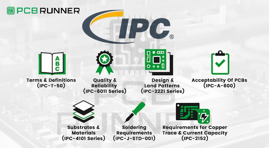
1. Terms And Definitions (IPC-T-50)

This standard includes and explains all terms and definitions that are relevant to PCB design and manufacture for communication purposes within the industry.

2. Design And Land Patterns (IPC-2221 Series)

The IPC 2221 series provides general design requirements, including effective land pattern design for the most economical board layouts.

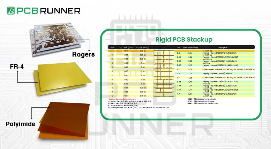
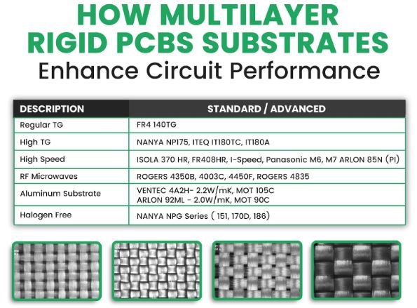
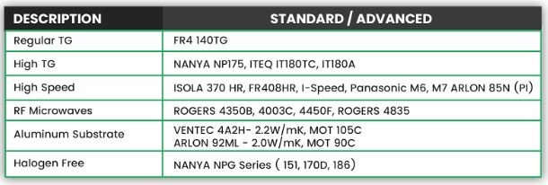
3. Substrates And Materials (IPC-4101 Series)

These standards describe the requirements for the PCB’s base materials and substrates, in selection for specific needs and criteria for different uses.

4. Quality And Reliability (IPC-6011 Series)

The rigid, flex, and rigid-flex boards have differing quality and reliability standards, and this overall standard sets criteria for those PCB types.

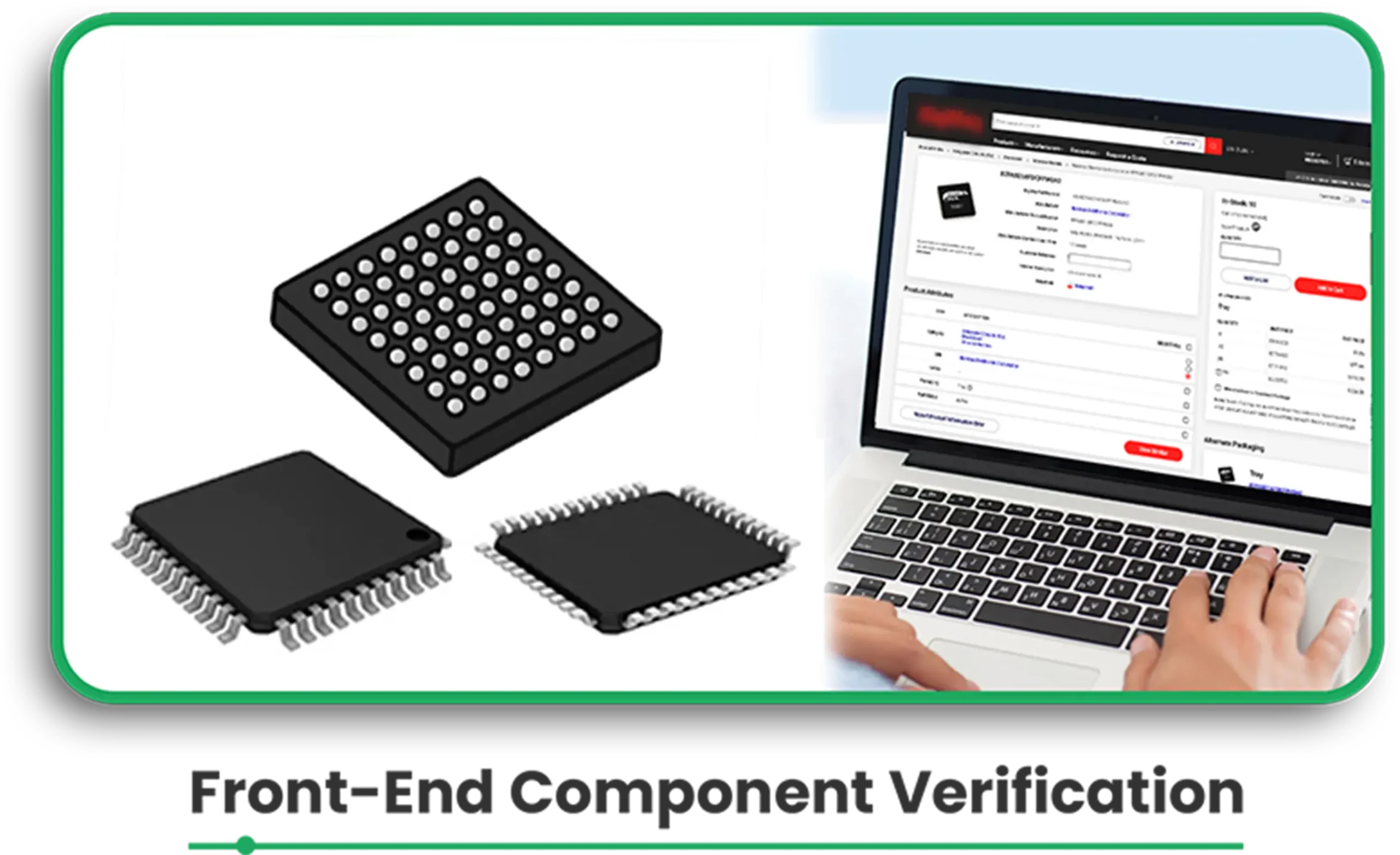
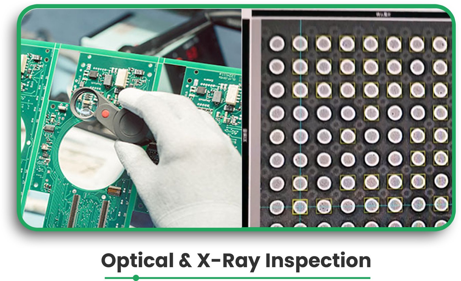
5. Acceptability Of PCBs (IPC-A-600)

This notably utilized standard intends to define the class of the PCB for its application and the acceptability requirements for completed boards.

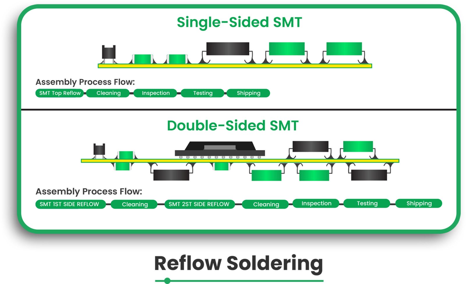
6. Soldering Requirements (IPC-J-STD-001)

This standard defines the requirements for soldered electronic assemblies in terms of materials, processes and workmanship.

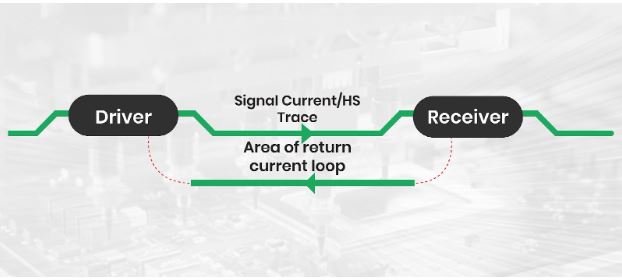
7. Requirements for Copper Trace and Current Capacity (IPC-2152)

This document outlines the execution of a specific current capacity trace to a PCB design. 

Use of IPC Standards in PCB Design and Prototyping

The application of IPC standards during the PCB prototype phase is critical to achieving the desired quality and performance in the final product. Manufacturers make IPC circuit board standards during design processes so that any evident flaws within the design can be resolved prior to manufacturing.

Expert Insights: Progress of IPC-7351 Standards

A study published on ResearchGate suggests that the design and specification of the IPC-7351 standard are set to supersede the old IPC-SM-782 Surface Mount Design and Land Pattern Standards. IPC-7351 makes necessary changes with respect to design and requirements for assembly and testing, including metric specifications for component dimensions and land patterns, since there are differing geometry requirements based on a product’s use case.

The document includes guidance levels for three standard land pattern dimension levels:

Level A: Exceeds for most digital electronics requiring soldering.

Level B: Moderate balance for more compact electronics.

Level C: Less protrusion for minimum compact electro-mechanical assemblies.

Employing this system of levels makes it possible for manufacturers to customize electronic assemblies and components for optimum efficiency and reliability.

Analysis of Other Industry Comparisons 

UL Standards 

What separates UL standards from others is their focus on safety solely, which is in contrast with IPC circuit board standards that focus on both quality and reliability. It is a lot more integrated in its approach. 

ISO Standards

ISO standards, like ISO 9001, focus on quality management systems without delving into specifics. These standards are too broad compared to IPC standards. Additionally, IPC standards focus on electronic assembly, which makes them ideal for the electronics sector. 

Benefits of IPC Circuit Board Standards

1. Improved Product Performance and Quality 

IPC standards take into account various operating conditions under which a PCB needs to function reliably. Therefore, Argus can maintain solid quality benchmarks. 

2. Uniformity and Flexibility 

Processes that are standardized reduce the chances of design errors and production inconsistencies. 

3. Better Interaction 

Collaboration between designers, manufacturers, and clients is more efficient due to shared standards and definitions. 

4. Cheap Production 

Rework and material waste have decreased, which, along with lean manufacturing, has made IPC standards cheaper to use. 

5. Pro-Environmental 

Many IPC circuit board standards define sustainable materials, which aids the use of pro-environmental practices. 

QAT and Quality Control Procedures Linked to IPC Standards 

Electrical Tests 

No particular assembly’s operational requirements are ignored, as the IPC standards set forth precise testing processes for all components of an assembly. 

Environmental Tests 

The endurance and thermal resistance of PCB products are tested under IPC standards for environmental testing.

Compliance with IPC Standards

Understanding the Standards 

To comply with the IPC standards, one must have a deep comprehension of the IPC standards. This means mapping standards to specific PCB projects. 

Implementation 

Achieving compliance with IPC standards at all levels of PCB design and fabrication activities is fulfilled from the first step to the final test procedures. 

Certification 

IPC certification confirms a company’s commitment to quality and reliability, enhancing trust and credibility with partners and clients. 

Conclusion 

IPC standards drive the dynamism and quality of the PCB industry. From developing the scope of PCB prototypes to ensuring compliance at volume manufacturing, these standards make a tremendous impact on the development of high-quality, reliable and efficient electronics. Through the electronic design and production cycle, one needs to follow IPC standards for circuit boards to remain competitive in the business and deliver electronic products that the market needs. 

The electronics industry is being forced to adopt new standards because of increased competition and changing market dynamics. Embrace IPC standards with PCB Runners to ensure that new products developed will be reliable, efficient, and environmentally friendly.

Maximising High-Speed Signal Transmission with Advanced PCB Reference Plane Techniques

PCBs of high speed are becoming increasingly important for modern systems and devices such as computers, smartphones, and telecommunications equipment that require high data transfer rates. To preserve the integrity and performance of the signal, the reference plane of a PCB has to be designed carefully. This blog aims at advanced techniques of high-speed signal transmission by optimizing the PCB reference plane design in addition to other design parameters for PCB circuit board manufacturers.

Maximising High-Speed Signal Transmission with Advanced PCB Reference Plane Techniques

Importance of Reference Planes to PCB Construction

A reference plane in a PCB acts as a stable voltage plane, typically a solid layer of copper, providing an essential grounding path for high-speed signals. When used alongside signal traces, reference planes are pivotal in shielding traces against electromagnetic interference (EMI).

Reference planes are crucially important in designs with differential pairs, which are used for high-speed interfaces like PCI-Express and Serial ATA. Signal pairs are plus-and-minus combinations of two signals that need a certain level of reference plane to preserve signal quality, limit noise, and improve transmission efficacy.

Problems Encountered in High-speed PCB Design

With the increase in demand for the integrity of high-speed PCB signals, designers of PCBs tend to have a growing list of problems to solve:

  • Complexity in Distribution of Power: Modern parts with multiple voltage levels have created cutouts in reference planes.
  • Impedance Changes: Changes in trace thickness, spacing of differential pairs, or nonuniform reference planes can result in severe signal reflections and information loss.
  • Electromagnetic Interference (EMI): Cuts in the reference plane can create undesired signals that contribute to a signal’s degradation.
  • Crosstalk: The coupling of adjacent traces can result in the loss of a specified signal.

PCB Reference Plane Design Guidelines

The following goals can help structure the PCB reference plane design for efficient high-speed signal transmission:

1. Solid, Uniform Planes

Do not allow cuts or gaps in the reference plane. Breaks in planes lead to signal distortion due to unstable impedance paths.

2. Efficient Use of Ground Layer

Ground planes should be placed next to high-speed signal layers in addition to signal layer loops. This configuration helps improve the quality of the signals while minimizing signal loops.

3. Differential Pair Routing Control

Traces should maintain equal spacing from the reference plane to help control differential pair routing. The above setup enhances impedance control and allows the reduction of signal suffrage.

4. Via Reduction

Reducing vias helps preserve high-speed PCB signal integrity, as each via discontinuity can have a distinct impact on high-speed signals. Where required, place them away from return paths to help maintain signal integrity.

5. Guard Important Signals From Interference

For traces with high EMI and crosstalk, it would be best to use shielding or guard traces to reduce interference in environments where noise is rampant.

6. Confirm The Results of The Impedance Computation

Employ simulation software for the network to compute, in addition to confirming the results pertaining to trace impedances and differential impedance, which is usually 100 ohms in high-speed situations.

Impact of Slits on Signal Transmission

Due to the advancement of multi-power designs, cuts in the reference plane are often necessary. Understanding the effects of these cuts on signal propagation is equally important in order to reduce negative consequences.

Experimental Findings

One of the effects noted was that the insertion of a 5mm slit in a microstrip reference plane resulted in a differential increase of approximately 6 ohms. The Sdd21 measures showed a significant recession of propagation signals when the common mode impedance (Zcom) was lower.

Within this study, the authors presented mathematical models to demonstrate how the effect of the slits. This information can assist designers when devising a plan to alter the design that seeks to enhance the transmission characteristics.

Primary Measurement Methods of High-Speed PCB Signals

For optimal Testing and Measurement, a high-end standard is followed by PCB circuit board fabricators. Some of these techniques include:

1. Time Domain Reflectometry (TDR)

TDR gives Time Domain Reflectometry the ability to reflect pulses from a line communication and perform analysis of transmission. To facilitate the interpretation of problem areas like slits in reference planes.

2. Transmission and Crosstalk Analysis

Broadband network analyzers do not measure transmission losses or crosstalk. This information is crucial in helping designers measure how different facets of the signal design affect its integrity.

3. S- Parameter Analysis

Static S-Parameter synthesis allows the Designer to perform S-Parameter simulation and pristine quality verification of Signal Transmission. This may also include suggesting alternatives to the existing assembly or routing novel transmission paths.

Practical Approaches to High-Speed Signal Integrity

The techniques to tackle PCB reference plane design disruption problems:

1. Stitching Capacitors

The introduction of stitching capacitors can solve the placement of slits or gaps. These slits and the stitching capacitors provide a routing low impedance during high frequencies.

2. Differential Pair Shielding

Employ shielding where routing of differential pairs across a slit is considered.

3. Simulation and Modeling

Use prediction tools to diagnose, anticipate, and rectify shortcomings before it is too late. Due to the introduction of simulation technologies, designers now have the ability to evaluate how modifications will affect the overall high-speed PCB signal integrity prior to the physical production stage.

4. Design Rule Checks (DRC)

Ensure that reference planes are relevant and consistent throughout the entire structure via thorough DRCs with special emphasis on high-speed signal design guidelines as supporting criteria.

Emerging Trends in High-Speed PCB Design

Newer devices and higher data rates must match technology’s evolution, requiring a more refined PCB design style. Advanced materials like low-loss laminates are rapidly emerging in the market for high-speed designs. Furthermore, engineers are solving the complex challenges of high-speed PCB signal integrity with the help of powerful simulation tools and artificial intelligence-based design optimization.

PCB circuit board manufacturers need to be at the forefront of innovation to stay competitive and provide advanced technologies.

Conclusion

To integrate maximum permittable signal transmission speeds in PCB designs, reference plane techniques need to be modified strategically. Consistency in reference planes, optimal routing of differential pairs, and rigorous testing are some of the steps that PCB circuit board manufacturers need to take to design for the modern high-speed world.

By carefully planning and following best practices, PCB circuit board manufacturers can overcome design challenges while achieving high-speed PCB signal integrity and effective performance in demanding environments.

Stay updated with such information at PCB Runners.

Materials for HDI PCBs

High-Performance Materials for HDI PCBs

High-density interconnect (HDI) PCBs have transformed the electronics world by making it possible to design smaller and more powerful devices. They are widely utilised in telecommunications, aerospace, automotive, and consumer electronics. 

These advanced PCBs’ ultra-high functionality and dependability are achieved through the use of high-performance materials and innovative solder mask materials. In this blog, we will focus on essential materials employed in the manufacturing of HDI.

The Role of Advanced Materials in HDI PCBs

Substrate Materials: Beyond Traditional FR4

Flame-retardant epoxy laminate FR4 was and still is the preferred base material for the majority of PCBs. However, due to the miniaturisation of devices and their increasing performance, FR4 has been found inadequate in various thermal and electrical specifications. Thus, the shift is taking place towards the usage of polyimide, PTFE (polytetrafluoroethylene), and ceramic-based substrate materials.

  • Thermal Stability: Ideal for use in extreme conditions, such as the automotive and aerospace sectors, Polyimide and ceramic-based substrates are able to operate under extreme environments.

Delamination

  • Electrical Performance: PTFE is a low-loss dielectric material with a low dielectric constant and dissipation factor, easily incorporated into 5G and superfast communication systems.
  • Miniaturisation: The ability to achieve intricate structures is possible due to advanced ceramic substrates with excellent mechanical strength and low thermal expansion, which can provide punctual and reliable performance.

Miniaturisation

These innovations make the next generation of electronic gadgets smaller, quicker, and more efficient than ever before.

Expert Insight: Advanced Materials for the Growing Needs of a PCB

Modern electronics are far too advanced to handle using older, outdated materials. This is specifically highlighted in the ResearchGate paper “Advanced Materials in PCB Manufacturing,” which includes this excerpt:

“Along with FR4, there were many materials above it that catered to a large number of applications but slowly, over the years, became irrelevant as devices started to shrink in size and outperformed the older models. The industry has now moved on to polyimide, PTFE, and ceramic-based substrates, which allow unparalleled thermal stability and durability while having blunt electrical components.”

Such developments are critical for industries that depend on compact size, high frequency, and high-speed communication as well as accuracy and reliability.

Conductive Materials: Reliable For Signal Transmission

At the moment, copper is the only material used in high-density interconnect PCBs since it is the most reliable and conductive. In dense layouts where more intricate designs are required, the copper on the micro vias and fine lines serve the purpose well.

Solder Mask Materials: Performance Protection and Improvement Enhancements

In HDI PCBs, the solder mask is one of the important layers to prevent damage from the environment, solder bridging, or contamination, as well as protect the device. The development of solder mask materials for high-density designs is crucial because they can maintain a high level of resolution and thermal stability.

Key Properties of Advanced Solder Masks:

  • Precision: Finer lines and spaces are critical.
  • Resistance: Endures degradation over several cycles of soldering.
  • Low Dielectric Values: Elevate the signal preservation in high-frequency uses.

The advancement of new solder mask materials with better thermal and electrical qualities is crucial.

Final Thought

The choice of advanced substrates, solder masks, and any additional components is essential for the high-density interconnect PCBs. Improved thermal control, enhanced electrical performance, and increased support for the miniaturisation of electronic components.

At PCB Runners, we take pride in using the newest materials and advanced manufacturing methods to create the highest-quality high-density interconnect (HDI) PCBs that exactly meet your needs. From advanced substrates to high-performance solder masks to other comprehensive PCB needs, we are ready to assist.

Reach out to us today to discover more about HDI PCBs and how we could assist your next venture.

FAQs

Q1: What are HDI PCBs?

A1: HDI Printed Circuit Boards (PCBs) have high wiring density relative to the surface area of the board, meaning they can link more components together at a time. They employ finer lines and spaces, reduced vias, and enhanced component density.

Q2: Why is material selection important in HDI PCBs?

A2: The materials selected determine the electrical performance of the PCB, the thermal management capability of the laminate, and the mechanical stability. These factors directly relate to the PCB’s reliability and functionality.   

Q3: What are the advantages of using advanced solder mask materials for HDI PCBs?

A3: The latest solder masks are less susceptible to damage from exposure to external elements while maintaining signal stability with excellent resolution, low dielectric constants, and high thermal stability.  

Q4: Why do advanced substrates enhance PCB performance?

A4: Advanced polyimide and ceramic substrates offer improved thermal and electrical performance, compact design support, and enhanced performance due to higher stability. 

Flexible PCBs for Flexible Displays

Flexible PCBs for Flexible Displays: Transformation of the Electronics World

Recently, there has been a significant introduction of enhanced features in consumer electronics—flexible displays. From curved televisions to foldable smartphones, the designs are sleek and offer some modern features.

Flexible Printed Circuit Boards (FPCBs) enable the core structure of these devices and their displays. In this blog, we’ll explore how flex and rigid PCB technologies are essential for modern, flexible displays and their benefits across industries.

What Are Flexible Printed Circuit Boards?

FPCBs, or flexible PCBs, are designed to bend without losing their electrical function. Unlike Traditional rigid PCBs, these are more modern and are crafted from substrates such as polyimide, which provide them with the needed shape.

Types of PCBs Used in Flexible Displays

Flex PCBs are ultra-flexible circuit boards used in devices that require folding, twisting, or curving features.

Rigid-Flex PCBs: The circuit board is made of a combination of flexible and rigid circuits. True to its name, it offers enhanced strength whilst maintaining adaptability.

Both types, as mentioned above, are widely termed compact and lightweight components.

The Importance of Flexible PCBs within Flexible Displays

A flexible display needs to have parts that are light in weight, compact, and effective. Conventional rigid PCBs cannot meet these specifications because of their inflexible structure. Flexible PCBs offer a solution because they have the following characteristics:

  • Bendability: The feature necessary for smartphones and mobile wearables.
  • Space Efficiency: FPCBs use less vertical space, making it possible for manufacturers to construct ultra-thin displays.

Space Efficiency

  • Lightweight Structures: This feature is beneficial for portable devices such as tablets and fitness trackers.

Lightweight Structures

  • Durability: Flex circuits perform consistently over time, even after repeated cycles obending.

Key Materials Used in Flexible PCBs

The kind of materials selected for flexible PCBs for displays determines the performance and reliability of the PCB.

Substrate Material:

  • Polyimide is the material of choice because of its flexibility and high thermal stability.
  • Polyester is also used for cost-sensitive applications, although it has a lower resistance to thermals.

Conductor Material:

  • Copper is widely used because of its good electrical conductivity.
  • Copper foils can be laminated with the polyimide flexible substrate to produce robust circuit traces.

Adhesive Layers:

  • Epoxy or acrylic adhesive serves as the conductive layer and the polyimide substrate adhesive.

Methods of Construction for Flexible PCBs

Building FPCBs aims to achieve flexible display capabilities, and the following procedures do it:

1. Cleaning and Preparing Substrate

The flexible substrate is cleaned and laminated with an adhesive layer and a protective coat.

2. Etching and Patterning

The Circuit patterns are created with Photolithography techniques, followed by excess copper removal through etching.

3. Application of External Circuitry

The multilayer integrated FPCB structure is constructed by laminating single circuits.

4. Plating and Drilling

Sequential plated through holes (Vias) are drilled for layering, and then electrical connections are plated to the Vias.

5. Quality Assurance and Testing

Flexible PCBs have high reliability and performance which comes from extensive testing as well as industry standard incorporation.

Usage of Flexible PCBs in Screens

The adoption of flex and rigid PCB technologies has remarkably increased, enabling their use in flex and bendable displays:

1. Smart Phones with Attachments

Flexible PCBs allow folding designs of displays as they bend around the corners seamlessly.

2. Smart Wearable Devices

FPCBs in smartwatches can be used because of their advanced ergonomic features.

3. Televisions with Curved Screens.

FPCBs are less fragile and the increase in display FPCBs allows for more broad usage in modern televisions.

4. Screens in Automobiles

The interface used in modern cars, with clusters and infotainment systems made with flexible FPCBs, has created customer-integrated curved displays.

5. Medical Devices

Today’s medical monitoring devices can be made smaller and more portable, owing to lightweight flexible PCBs that can adapt to a variety of displays.

Advantages of Flexible PCBs for Display Applications

Integrating FPCBs into flexible displays has many benefits:

  • More Productive: Allows for diversity in the shapes of devices.
  • Increased Reliability: Endures bending and moisture.
  • Lowered Difficulty for Assembly: Reduced use of connectors and interconnects lowers assembly time.
  • Electrically Efficient: Shorter signal paths enhance electrical performance.
  • Financially Convenient: Reduced material usage and compact designs lower production costs.

Challenges and Solutions

There is always a price to pay for certain benefits, in this case, the manufacturing process of FPCBs for flexible displays:

1. Material Handling

Challenge: The flexible substrates are easily breakable and unsightly to deal with.

Solution: Use of automation and specialized handling tools for effective placement.

2. Signal Integrity Issues

Challenge: Signal loss from older traces.

Solution: Careful design and impedance control can help reduce signal losses.

3. Heat Management

Challenge: Slender devices have less surface area to cool off.

Solution: Using thermal vias and heat-dissipating materials.

Expert Insights

FCBs, or Flexible Circuit Boards, are vital components in contemporary electronics systems. They are present in mobile phones, laptops, smartwatches, cameras, and even robotic arms. These circuit boards are especially beneficial in applications with constrained spaces where standard Printed Circuit Boards (PCBs) cannot be utilized.

In comparison to conventional PCBs, FCBs possess several advantages like increased reliability, decreased weight, and more space efficiency. Nevertheless, they come with certain challenges, particularly during the installation and repair procedures of a system. During installation, FCBs are stressfully bent at multiple points which is significantly more than rigid PCBs. This stress, which gets compounded due to the system’s repeated bending, eventually leads to breakage.

The complexity increases when it comes to FCBs because of their structure and the requirement to model both the installation and operational phases of the model. Thus, in this study, a methodology for modelling these phases was created using Ansys Mechanical. The simulation determined the stresses induced during both phases and assessed the fatigue life of the FCBs after the operational phase. 

Two types of models were studied: a Rigid-Flex PCB, which consists of a flexible circuit between two rigid PCBs, and a Flex FCB cable with no rigid components. For both models, shell elements were used to mesh the thin FCB structures, which rotate and bend significantly and are therefore subjected to large loads.

Trace mapping streamlined the intricate geometry of vias, solder connections, wires, and other electronic CAD components. This technique modelled the geometry as dielectric layers and mapped the metal fraction onto these layers so that the effects of the traces were accurately modelled. The models were bent at an angle of 180 degrees in order to study the fatigue due to this bending load. 

For the FCB cable, there was some additional stress analysis conducted during the installation phase, because the stresses developed at this stage do have an overall bearing on the fatigue life of the cable. Rigid surface bodies were utilized in the simulation to deform the FCB cable into its final installed position to model real-world conditions.

This research also performed a High-Performance Computing (HPC) scalability analysis to provide optimal simulation performance. This analysis, in turn, determined the appropriate division of the processor cores against the time necessary to reach an accepted solution. This made it possible to simulate the model faster and more efficiently.

This study enriches knowledge of FCBs’ behaviour during the installation process and operation. In addition, it serves as an accurate predictor of performance and fatigue life, enabling engineers to design more effective FCBs for different electronic purposes. By preemptively spotting certain failure modes, the methodology increases the reliability and lifespan of these important components.

Conclusion

Flexible Printed Circuit Boards (FPCBs) are changing the landscape of display technology, bringing advancements such as flexible smartphones, curved TVs, and other smart wearable devices. The fusion of flex and rigid PCB technologies allows manufacturers to satisfy the increasing market need for multifunctional electronic devices. Anticipating future trends within the industry, FPCBs will be the basis for advanced next-generation displays for many years to come.

PCB Runners is a leader and supplier of high-quality flex and rigid PCBs for various applications across several industries. With our experience and reputation, we provide dependable and affordable PCBs specifically designed to meet our customers’ needs.

Frequently Asked Questions

Q1: What are flexible PCBs used for?

A: Foldable smartphones, wearable devices, automotive displays, and medical devices all utilize flexible PCBs due to their lightweight nature and easy adaptability.

Q2: What materials are used in FPCBs?

A: Polyimide substrates, copper conductors, and protective solder masks are commonly used materials.

Q3: What is the difference between flex and rigid PCBs?

A: Flex PCBs are adaptable to bending and twisting, whereas rigid PCBs have no flexibility. Rigid-flex PCBs offer the best of both worlds.

Q4: What challenges are associated with FPCBs?

A: Advanced material handling, signal integrity concerns, and thermal control are the major challenges with FPCBs. However, advanced manufacturing techniques can solve these problems.

Q5: Why choose PCB Runners for flexible PCBs?

A: When it comes to flex and rigid PCBs, PCB Runners has unmatched industry experience, top-tier materials, and specific peripheral solutions.

Designing Military-Grade PCBs

Designing Military-Grade PCBs For Maximum Durability

Military active PCBs (printed circuit boards) need to pass grueling tests to endure the straining conditions of a theater of war and work effortlessly. The high working temperature, vibrations, and even moist conditions are some of the hurdles these specialized circuit boards need to overcome. 

This blog will discuss the strategies employed by leading PCB manufacturers to fabricate military-grade circuit boards with exceptional strength and toughness.

What Makes a Military Circuit Board Different?

As opposed to standard PCBs, military circuit boards need to operate flawlessly even in extreme conditions like rapid/ sudden changes in temperature, exposure to certain chemicals, and high-amplitude vibrations. To cater to these unusual demands, military PCBs are designed following strenuous requirements like IPC Class 3 and MIL-PRF-31032.  

The focus lies on selecting materials, design techniques, and manufacturing processes that offer the best reliability. Also, circular shape requirements have broadened the applicability of circuit boards in the military field.

Key Materials for Military PCBs

For a military-grade PCB, high-performance materials that can resist overpowering heat, chemicals, and even mechanical strain are essential to support. Some common materials are: 

High-Tg Laminates: Isola FR408HR and DuPont Pyralux are specified materials that resist temperatures over 200 degrees Celsius.

high tg

Metal Core Substrates: Aluminum and copper cores aid in the rapid dissipation of heat.

Metal Core Substrates

High-Frequency Materials: High-frequency signals are well handled by materials such as the Rogers 4000 series. 

Expert Insights 

Military-grade PCBs have some of the toughest standards in electronics. The PCBs must endure severe conditions, function well under stress, and be capable of continual operation without any failure. 

One of the strictest standards for these boards is MIL-PRF-31032, which covers everything global boards fail to defocus on. Everything from the design of the PCB, the material chosen, and even the method of manufacturing is set in stone. But it doesn’t stop there- military standards define the set components that leave very little breathing space. 

Moreover, there are regulations outlined that govern entirely the assembly of the boards. Quality control guidelines are also elaborated to check that the set high-performance thresholds are met.

Thermal Properties: The Importance of Tg

The glass transition temperature (Tg) is crucial for military PCBs. It represents the temperature beyond which the material softens, losing its rigid structure. For military applications, designers recommend materials with a Tg of at least 170°C to 200°C or higher.

Material Type Tg Range
Low Tg 130°C – 160°C
Medium Tg 160°C – 200°C
High Tg 200°C +

Top Design Rules for Military PCBs

Here are essential design considerations when creating a military circuit board:

1 Surface Mount and Land Considerations

  • Defects on the sides of rectangular lands should not exceed 20%.
  • Lands for circular mounts (BGAs, for example) should strive to have minimal defects, ideally below 10 percent of the circumference. 

2. Porous Plating Method Hole Specifications

  • For the required thickness, copper plating should be a minimum of 80% of the thickness. 
  • Voids in the plating should not be more significant than 5% of the PCB thickness. 

3. Via Copper Plating 

  • For filled vias, there should be no voids or bumps that can give access to internal layers. 
  • Moisture damage will be prevented with proper copper plating of vias. 

Additional Tips for Designing Durable Military PCBs

Use heat compounds and heat-resistant enclosures to control excessive heat. 

  • Component Isolation: High, more sensitive components should be placed away from low-frequency parts to minimize interference. 
  • Simulations before Layout: Simulations should be done to measure performance in real-life situations. 

Clock signals should be covered with aluminum shields to limit interference. 

The use of chemical resistant and anti-moisture conformal coatings can be used to shield the components. 

The Role of Circular Circuit Boards in Military Applications

Due to their compact, efficient features, circular circuit boards are becoming increasingly prevalent in military applications. These boards have a lot of advantages, such as: 

  • Space Efficiency: These are essential to installations that need compact electronic integration. 
  • Concise Signal Traces: The radius of the board reduces trace lengths, thus enhancing performance. 
  • Mechanical Strength: Because of their unique shape, mechanical stress is evenly distributed, giving them strength. 

Choosing the Right PCB Manufacturer for Military Circuit Boards

To ensure compliance with military specifications, select ITAR-registered PCB manufacturers.

  • A reliable PCB partner should: 
  • Abide by the IPC and MIL standards. 
  • Have the necessary equipment to manufacture multi-layer and circular circuit boards. 
  • Conduct adequate tests and quality control measures. 

Here at PCB Runners, we focus on military-grade PCB manufacturing, emphasizing quality, durability, and precision to satisfy the toughest requirements.

Conclusion

Achieving a military-grade PCB means stricter policies on materials used, layout design, and standards set. And with any circuit board, be it traditional or circular, strength and dependability come first. No question, working with a reputable PCB manufacturer guarantees that your military circuit boards will work in the most demanding situations. 

If you need a PCB manufacturer who is sensitive to the intricacies of military applications, PCB Runners is your perfect solution. 

Reach out today to find out more about our services for custom military circuit board construction. 

FAQs 

What are military circuit boards? 

Military circuit boards are specially designed PCBs that can sustain extreme conditions, such as high temperatures and powerful mechanical forces. 

What materials are used for military PCBs? 

Commonly used materials include high-Tg laminates, metal core substrates, and high-frequency Rogers 4000 series. 

Why are circular circuit boards used in military applications?

Circular circuit boards can save space, enhance the efficiency of signal paths, and improve the distribution of mechanical stress. 

How do I select a suitable PCB manufacturer? 

You should seek out ITAR-registered manufacturers that specialize in military-grade PCBs and have a strong compliance record with IPC standards. 

Which standards are military PCBs subjected to? 

These include, among others, the seminal MIL-PRF-31032 and IPC Class 3, which guarantees quality and reliability in the design and construction of the PCB for military purposes.

Achieving Higher Accuracy In Multilayer PCB Testing with X-Ray Inspection

The integration of electronic components into a single device has escalated the need for dependable multilayer printed circuit board (PCB) testing. These boards serve as the foundation for contemporary electronics, containing complex connections and components within several layers. 

The operation of these devices is fault-free only after adopting sophisticated testing methods. Automated X-ray inspection (AXI) is increasingly being used and has developed into an essential gear for testing these devices upon completion. This article highlights how automated x-ray inspection PCB performs, its benefits, and how it allows for stringent control of checks.

automated x ray inspection pcb

The Complexity of Multilayer Printed Circuit Boards

Multilayer PCBs are key to most advanced applications, such as telecommunications, aerospace, automotive, and even healthcare devices. With several conductive layers encased in insulating material, these boards have improved function and performance. However, the level of sophistication of these boards brings forth problems during the manufacturing stage. These problems include hidden solder joint defects, component misalignment, and via-incomplete stages.

Advanced testing techniques such as optical inspection and electrical testing seek to overcome these challenges. Unfortunately, neither approach is adequate for addressing the possible multilayered internal defects hidden inside the PCB. Hence, automated X-ray inspection PCB can prove to be a significant advancement in the industry.

How Automated X-Ray Inspection PCB Works

AXI systems harness high-energy X-rays to penetrate through and reveal the internal structures of a PCB. Unlike visual inspection, which only looks at the surface, X-rays can expose hidden defects located within the board’s layers. These systems create sophisticated images displaying the quality of solder joints, the placement of components, and other possible defects.

Typically, the procedure consists of the following stages:

How Automated X-Ray Inspection PCB Works

  • Image Acquisition: Capturing images at pre-defined angles using X-ray projection on the PCB.
  • Data Interpretation: Using X-ray imaging to perform defect recognition with artificial intelligence algorithms.
  • Defect Recognition: The system captures voids, missed alignments, and solder bridging as problems highlighted by the system.

AXI is especially effective in discovering defects in Fine-Pitch Components and High-Density Interconnects (HDI) because those flaws are difficult to see with the naked eye.

Expert Insights: Enhanced Testing Techniques

As noted in an article from ResearchGate, older X-ray techniques such as Digital Radiography (DR) often struggle with multilayer printed circuit board testing. Overlapping images provided by DR makes patient diagnosis very challenging since it becomes impossible to view every layer distinctly or to find clear defect locations.

To overcome the previously described issues, the study proposes an innovative technique that uses the following steps:

  • Oblique Angle Irradiation: The surface of the PCB is irradiated with X-ray at an angle that is not perpendicular to the surface.
  • Rotational Projection Imaging: The board undergoes rotation while projection images are taken.
  • Slice-by-Slice Reconstruction: Each layer of the image is constructed from detailed cross-sections revealing pertinent information for every single component of the target object.

This approach remarkably boosts the overall accuracy of defect analysis and provides insight into the construction of the PCB’s internal layers.

Advantages of Multilayered PCB X-Ray Inspection

1. Non-Destructive Testing

The primary benefit of automated X-ray inspection PCB is completely damage-free inspection. Manufacturers can examine PCBs without the risk of inflicting any damages that would hinder repair or rework.

2. Enhanced Defect Detection

A very diverse number of defects can be widely identified using X-ray inspection, including but not limited to:

– Voids in solder joints.

– Missing or misconfigured components.

– Inadequate or improperly constructed vias.

– Short circuits or solder bridges.

3. Improved Quality Control

X-ray inspection reduces defect and scrap rates, resulting in improved overall product reliability by catching mistakes earlier in the production cycle.

4. Automation for Efficiency

Quality remains high while meeting the demand of a high volume of production due to rapid and accurate testing provided by automated X-ray systems.

5. Layer-Specific Analysis

Other techniques than traditional methods offered detailed layer-specific analysis and the ability to gain insights not previously accessible. This research gate study has covered the machine learning reconstruction method, for example.

Use of PCB X-ray Manufacturing Process

Xray technology, particularly AXI, is used at almost all stages of PCB manufacturing:

  • Prototyping: A step that validates that a design does not have any glaring mistakes at the start.
  • Mass Production: Doing production in bulk with a guarantee of consistency in the quality of output.
  • Defect Investigation: Determining the reasons and failure parts for the PCBs found to be defective.

Aerospace, telecommunications, and automotive industries are big users of the technology due to established quality requirements.

From Supreme Materials to PCs: Testing with a Challenge

As bulk production of PCBs becomes commonplace, testing becomes increasingly challenging, which is one reason why advanced materials have to be properly tested. As devices become smaller and more powerful, materials like solder masks and high-frequency laminates create big problems.

AXI systems will have to change to improve the materials that can be inspected on judgeable terms. Quality monitoring and check-ups of non-conductive or super-dense layers will be the basic requirements for ensuring quality maintenance.

New Agendas in Xray Inspection Technologies for PCBs

1. 3D X-Ray Imaging

Level and volumetric data that can be attained with newer 3D X-ray technologies allow for extremely accurate analysis of complicated structures.

2. AI Based Analytic

Along with more profound levels of scrutiny, the use of artificial intelligence and machine learning for automated X-Ray Inspection systems in ramping up deficiency distinctions, while keeping the rate of false alarmers in check.

3. Smarter Automation

Improvements in automation will be made in future systems, further boosting the inspection speed while minimizing the need for operator involvement.

Conclusion

Methods such as automated X-ray inspection (AXI) are necessary. To achieve higher precision in multilayer PCB testing, TX-ray inspection nondestructively examines the internal structures of modern PCBs, which determine the reliability and functionality of contemporary electronic devices.

PCB Runners is a well-known provider of comprehensive PCB solutions and offers design, manufacture, and testing services. Our experience in multilayer PCB production and new inspection methods guarantee that our customers receive dependable, high-quality products.

Give us a call today to discover how we can assist your next project by utilizing these advanced PCB solutions.

FAQs

1. What is a multilayer printed circuit board?

A multilayer printed circuit board (PCB) has more than one conductive layer with insulating materials in between the layers; these PCBs offer enhanced functionality for more sophisticated electronic devices.

2. What exactly is automated X-ray inspection (AXI)?

AXI helps visualize the internal structure of PCBs using X-rays, which makes defect detection easier as defects are concealed within the assembly structure, hence improving the quality of the product.

3. Why is multilayer PCB’s X-ray inspection so important?

X-ray inspection can capture defects obscured by external layers and is necessary for ensuring product reliability and high endurance performance.

4. What do you think the defect AXI can reveal?

AXI can detect voids in solder joints, misplaced components, incomplete vias, and short circuits.

5. What goes into the maintenance of quality in multilayer PCB production provided by PCB Runners?

Runners PCB uses the latest inspection efforts, like AXI, to keep its quality standards at a high level and produce reliable PCB solutions.

How Multilayer Rigid PCBs Substrates Enhance Circuit Performance

Introduction

As the world becomes more industrialized, the need for high-performance circuits has increased significantly in the telecommunication, automotive, and IoT industries. The need for improvement has made multilayer rigid PCBs common since they provide an easy and effective way to improve a circuit’s performance. 

These advanced substrates enable designers to enhance components’ density and electrical and thermal performance and effectively allow for improvement in performance. 

This blog will discuss the multi-layered rigid PCBs’ contribution towards better circuit performance with an emphasis on signal integrity, thermal performance, and mechanical strength.

Also, we will discuss the ways multilayer rigid PCBs can enhance your designs for high-performance applications. 

How Multilayer Rigid PCBs Substrates Enhance Circuit Performance


Table

What are Multilayer Rigid PCBs? 

A Multilayer PCB with rigid construction consists of a stack of conductive layers separated by insulating substrates. The construction allows for more routing options for the signal within a compact space. 

These PCBs improve the connection density and functionality by integrating different layers together with more materials, such as FR-4, a fire-retardant fiberglass epoxy, for reliability and durability. 

With multiple layers, the signal integrity is significantly improved because the chance of interference and signal loss is greater over long distances. 

Key Properties of Multilayer Rigid PCBs. 

Electrical Properties: 

  • Dielectric Constant: It is one of the properties of signal integrity. Low dielectric constant materials such as FR-4 and others are often preferred for high-frequency applications because these materials have low dielectric constant. 
  • Dissipation Factor: It is one of the thermal properties of a low dissipation factor material, which helps minimize energy loss in the PCB material and improves the circuit’s efficiency. 

Thermal Properties: 

  • Glass Transition Temperature (Tg): The Tg value determines a material’s thermal stability. A material’s ability to withstand thermal damage is greatly dependent on its Tg value. 
  • Thermal Conductivity: It is important to manage heat in circuits with high-power components. Multilayer PCBs have better thermal management because they are designed to dissipate heat more effectively.

Mechanical Properties:

  • Peel Strength: The peel strength between copper and dielectric layers ensures that the adhesive bonds maintain structural integrity and durability during service.
  • Flexural Strength: Flexural strength ensures that multilayer PCBs endure stress or bending forces, which is very useful for portable devices and many rugged applications.

Materials

Benefits And Advantages

The electrical inclusion of multilayer rigid PCBs in electronic designs offers several benefits that improve circuit performance:

  • Improved Signal Integrity: The use of multilayer PCBs reduces the requirement of long and extensive traces, which cause signal loss and interference. This is critical in high-frequency circuits where signal integrity is a priority.
  • Better Thermal Management: With more layers to dissipate heat, multilayer PCBs can use high-power components without overheating. This is very important in devices with intense performance requirements, such as smartphones and automotive electronics.
  • Enhanced Miniaturisation: More components can be integrated into one compact board so that multilayer rigid PCBs enable smaller devices without performance degradation.

Expert Insights

The rigid flex multilayer PCB technology permits the use of fewer connectors and large harnesses for the interconnection of functional electronic systems. It increases the performance and makes it less complicated to handle packaging for high-durability space electronic systems while weighing and taking up less space for the modules. 

Here, only adhesive-free all-polyimide flexible laminates core, and no-flow glass-polyimide prepregs are utilized. A new process technology is introduced in this work to address manufacturing challenges like registration, coverlay protrusion on rigid areas, and residual copper left at the flexible and rigid junctions. 

Science has been worked out and implemented after determining the right combination of flexible, rigid, and low-flow prepreg materials. 

FAQs

Q1: What is the difference between single-layer and multilayer PCBs? 

Multilayer boards incorporate more than two conductive traces, enabling them to connect to other boards. This makes the signal stronger than on a single-layer board. 

Q2: Why is thermal management important in multilayer PCBs? 

Multilayer PCBs carry high-power components, which generate a lot of heat and require proper thermal conductivity to operate effectively without damaging the delicate components within the device.

Q3: In what ways do multilayer rigid PCBs positively improve signal integrity? 

Using multilayer PCBs helps shorten signal traces while encapsulating them inside layers to reduce signal interference and losses, which is significant in high-frequency circuit scenarios.

Q4: Do multilayer rigid PCBs have a greater budget than single-layer PCBs? 

Yes, multilayer rigid PCBs are usually more expensive because of the extra layers and construction means; however, they are far superior in outperformance and compactification.

Conclusion

Multilayer rigid PCBs are instrumental in improving circuit performance. They provide better signal integrity than single-layer PCBs, efficient thermal management, and mechanical robustness. These unique features enable their utilisation in the most advanced systems, including telecommunications, automotive, and IoT.

Take a look at our multilayer PCB solutions for increased efficiency and performance in your designs. Also, remember to subscribe to the latest updates in PCB technology and design.

PCB Assembly

From Design to Production: The PCB Assembly Process Simplified

Turning abstract designs of printed circuit boards (PCBs) into real, working products involves many tasks and requires attention to detail. This intricate process is something that both engineers and PC board manufacturers focus on to ensure seamless functionality.

PCB Runners specializes in printed circuit assembly, which has become a central activity for the company as it enables quick, dependable, and effective assembly of PCBs according to the drawing provided and functional specifications. 

We will simplify the PCB assembly process by designing the board assembly and then the case. If you are looking to make new prototypes or limited series, this is a good starting place, significantly to gain a better perspective of the steps involved. 

PCB assembly is an important aspect of consumer, medical, automotive, and industrial electronics, as it is used in key industries.  

Understanding these processes will aid those working on them in achieving high-quality production efficiently.

Key Information  

The entire process of assembly technology is captured in this diagram sequentially. Below are the steps on how it is performed: 

Step 1: Uploading Data/ Images of the PCB 

eC-smart tools such as the PCB Visualizer have enabled engineers to check their designs before the assembly phase commences. 

The company has to upload the images of the bare board for processing. 

Uploading data

Step 2: Uploading BOM and CPL Files 

The BOM (Bill of Materials) includes all component items, such as part number, description, and packaging. 

The Component Placement List (CPL) describes the location of all components on the board. 

bom

Step 3: Component Sourcing and Ordering 

An integrated system scans the BOM against the database of over 205,000 components to look for stock coverage. 

If components are not stocked, they need to be ordered from reputable suppliers through integrated APIs. 

Component Sourcing

Step 4: Front-End Component Verification 

For mounting, the correct placement, polarity, and type of package to be used against the PCB footprint are verified. 

Special requirements for mounting are determined and corrected in this phase.  

Step 5: Kitting and Component Preparation 

Items are arranged in feeders for better organisation, ensuring that they are loaded into the pick-and-place machines efficiently. 

Kitting & Component

Step 6: Solder Paste Application 

Until this phase, jetting or SMD stencil printing performs solder paste application to the PCB surface. 

A solvent paste inspection (SPI) carries out the cure check to determine the paste’s adequacy for the ensuing procedure.

Solder paste

Step 7: SMD assembly: pick & place

SMD components are positioned on the board automatically by pick-and-place machines. 

Thus, vision cameras inspect components for their sizes and angle position. 

Smd assembly

Step 8: Reflow Soldering 

The board is passed over a reflow oven, which helps melt the solder paste into a solid state, creating an inlet electrical connection to the components and PCB pads. 

Reflow Soldering

Step 9: Optical and X-Ray Inspection 

PixPect optical inspection scans the board for defects and correlates the image with properly scanned sheets. 

3D X-ray inspection can (with Nikon) detect concealed soldering connections and check the building quality of BGAs and LGAs components. 

Optical & x ray inspection

Step 10: THT Component Soldering 

Through-hole ones are assembled by means of selective soldering machines or manual soldering techniques

THT

Step 11: Final inspection and cleaning 

The final inspection should make sure that the assembled board is suitable for the design specifications. 

Before shipping, the board is cleaned, and all defects are corrected. 

Final Inspection

Benefits and Application 

Step by step understanding of the PCB assembly enables one to undertake the following actions: 

  • Enhancing Quality Control: By ensuring validation checks at many processes, the chances of committing errors are greatly minimized. 
  • Facilitate AI Methods: Integrated systems like automated component ordering and solder paste dispensing help to achieve quick turnarounds. 
  • Guarantee Component Fitting: Employing tools like PCBA Visualizer guarantees that components are placed and fit in accordance with the PCB’s design. 

By following the above guidelines, accurate, high-quality PCBs are produced with shorter lead times, making it an essential resource for PC board manufacturers seeking efficiency in production.

Expert Insights:

The following information is mentioned in the PCB Design Tutorial by David L. Jones.”

Many people start designing a PCB by placing all the components where they think they’ll fit best right away. While this approach might work for simple circuits, it’s not ideal for more complex designs with hundreds of components and multiple functional blocks. 

The main reason is that you can quickly run out of “routing space,” which is the space needed to lay down all the tracks (connections). If you fix the positions of all components first and then try to connect them, you may find yourself stuck and unable to route some connections. On the other hand, if you space the components too far apart, you may end up with a large board that wastes space and increases PCB board manufacturing costs. 

An inexperienced designer’s board often has evenly spaced components but messy tracks and vias (holes for connections) crisscrossing all over. This kind of design might work, but it’s inefficient, unattractive, and more expensive to produce. 

The best way to start is by placing all the components on the screen first. If you’re using a schematic design tool, you can import the design into your PCB program to automatically place the components. If you’re only using a PCB program, you’ll need to select components from the library and place them manually. 

Once all the components are on the screen, you can assess whether they’ll fit within the size and shape of your board. If the fit is tight, you’ll need to position the components carefully to save space and keep the routing efficient. 

If you have plenty of space, you can be more flexible with your layout. However, if the components don’t fit at all, you’ll need to revisit your design and adjust. 

FAQs 

What files do I need for PCB assembly? 

To ensure smooth printed circuit assembly, you need to upload the bare board data, BOM (Bill of Materials), and CPL (Component Placement List)

What is the purpose of solder paste inspection (SPI)? 

SPI ensures that the correct amount of solder paste is applied to the PCB pads, which is critical for proper soldering and component attachment. 

How does the pick-and-place machine work? 

The pick-and-place machine automatically picks up SMD components and places them onto the PCB, ensuring precise component placement. 

What is selective soldering? 

Selective soldering is a technique for attaching through-hole components to the PCB. It ensures precise solder joints without affecting nearby components. 

Why is X-ray inspection necessary in PCB assembly? 

X-ray inspection is essential for checking hidden solder joints, particularly for difficult-to-inspect components like BGAs (Ball Grid Arrays) and LGAs (Land Grid Arrays). 

Conclusion  

The PCB assembly process involves a series of well-coordinated steps that ensure the final product is functional and high-quality. From design verification to component sourcing and final inspection, every phase plays a vital role in producing reliable PCBs. 

By understanding this comprehensive process, both engineers and PC board manufacturers can make informed decisions that lead to faster production times and more cost-effective solutions for prototypes and small series production.

Essential Prototyping Techniques for High-Frequency PCBs

Introduction

Prior to constructing high-frequency printed circuit boards (PCBs), it is crucial to create a prototype. Such PCBs have applications in telecommunications, aerospace, and medical devices, where quality and operating efficiency are important areas of focus. Having a dependable and accurate PCB prototype helps resolve most of the potential problems before bulk production begins.

Low Frequency Signal Vs. High Frequency Signal

In this article, we explore the critical prototyping techniques used in the development of high-frequency PCBs, the impact of best practices, and innovations in design and performance, such as rigid-flex PCBs.

Essential Prototyping Techniques for High-Frequency PCBs

Here’s What You Need To Know

Concepts of Prototyping on High-Frequency PCBs

The following is what to look out for when prototyping a PCB of a high frequency:

  • Choose A Material: Opt for Rogers laminates, which are low-loss dielectrics, to reduce signal strength and impedance variations.
  • Control the Impedance: It is critical to maintain consistent impedance to avoid signals reflecting back and losing integrity.
  • Optimize Layer Stackup: The PCB design must consider the structure of layers to control EMI and lessen crosstalk.
  • Optimize Vias: Employ blind, buried, and micro vias to reduce parasitic inductance.
  • Routing Traces: To improve signals, use controlled-impedance traces with matched lengths, reduced bends, or avoided right-angle bends.
  • Thermal Management: Heat dissipation techniques should be utilized to improve high-frequency circuit stability.
  • Test and Validation: Obtaining an accurate performance read with TDR and VNA guarantees enhanced testing techniques.

High Frequency PCB

Benefits and Application

The following are the salient features of this section’s focus on prototyping techniques for high-frequency PCBs.

  • Improved Signal Integrity: Misbalanced impedance and poor routing of traces heavily distort signals and cause them to be lost.
  • Reduced Development Costs: It saves time and resources if flaws are spotted early in the design stage.
  • Enhanced Design Flexibility: Rigid-flex PCB designs increase constructional load but make the board lightweight and compact, which is helpful in fast-moving scenarios.
  • Scalability: A properly designed PCB prototype can transition effortlessly with few alterations to mass production.

By applying these techniques, engineers can create more affordable but dependable high-frequency PCB designs that satisfy the industry’s requirements.

Expert Insights

Designing embedded systems with high-frequency components involves several complex challenges, particularly when incorporating both analog and digital signals. Mixed-signal design issues, such as signal integrity, power integrity, and electromagnetic interference (EMI), are common in systems with components like WiFi, BLE, or Ethernet interfaces. \

To tackle these, board designers must focus on key aspects like stack-up design, component placement, and routing. The goal is to isolate high-frequency digital and analog signals, ensuring that they do not interfere with each other, particularly when dealing with RF functionality. 

Proper grounding and isolation of different sections within the PCB layout can minimize crosstalk and signal degradation, leading to more reliable and efficient designs. Furthermore, a high-layer count stack-up is often necessary to accommodate both high-speed digital interfaces and analog components, ensuring impedance control and power integrity.

In addition to the foundational design considerations, designers must pay close attention to the routing of high-frequency signals. Techniques such as coplanar waveguide routing and stripline routing on dedicated layers can prevent interference and ensure signal quality. It is also essential to track return paths carefully and keep RF interconnects isolated from digital components. 

Evaluating the design using advanced tools like field solvers before prototyping can help detect potential issues with signal and power integrity. These tools calculate crucial parameters such as impedance matching, network parameters, and radiated EMI, ensuring that the final design meets high-frequency performance standards. 

By addressing these challenges early in the design process, engineers can create high-performance embedded systems with seamless analog and digital integration.

Frequently Asked Questions

1. What materials work best for high-frequency PCBs?

For instance, Rogers, Isola, and Taconic laminates are all capable of providing low dielectric loss and stable performance at high frequencies.

2. What steps do I take to achieve controlled impedance on my PCB sample?

Accurate trace width calculations, the controlled impedance stack-up technique, and simulation software achieve controlled impedance.

3. Why would one opt for rigid-flex PCBs in high-frequency operations?

The design is favored for compact designs, superior signal quality, and superior resistance to harsh environments.

4. In what ways are via configurations relevant to PCB high-frequency performance?

Vias should be properly placed and selected (blind, buried, or micro vias) to reduce signal loss and other parasitic effects.

5. Is there a benefit to building a thermal prototype?

Adding thermal vias, heatsinks, and specific components can greatly help manage heat.

Conclusion

Mastering essential prototyping techniques for high-frequency PCBs is vital for achieving optimal performance and reliability. Whether you’re working on RF applications or high-speed digital circuits, paying attention to material selection, impedance control, and testing ensures a successful outcome.

Looking to enhance your PCB prototyping process? Explore our advanced solutions or contact us for expert assistance!

The Impact of Counterbore vs Countersink on PCB Performance

The Impact of Counterbore vs Countersink on PCB

When designing printed circuit boards (PCBs), it’s essential to understand how different hole configurations impact performance, including counterbore and countersink holes. Each of these types of holes has distinct characteristics that affect fastener placement, board strength, and board integrity. This blog explains when and how to use counterbore or countersink holes on PCBs.

By the end of this blog, you’ll learn how each kind of hole affects your PCB’s durability and assembly process. Whether you are an expert PCB designer or a hobbyist, understanding these differences will optimize your design. We’re also sharing tips on when to use each hole type.

Counterbore vs Countersink on PCB

Differences Between Counterbore and Countersink Holes

Feature Counterbore Holes Countersink Holes
Shape Straight cylindrical walls, flat bottom Conical, tapered shape
Function Allows fastener heads to sit flush with the PCB Enables screws to sit flush with a slanted surface
Opening Size Larger than screw diameter Tapered opening size, gradually narrowing
Shear Strength Higher shear strength due to vertical walls Lower shear strength, especially in high-load applications
Material Removal Less material removed, preserving strength Requires more material removal

Counterbore vs Countersink on PCB

When to Use Each Type

Counterbore Holes:

  • To hold heavier pieces of components in place
  • Use them in heavy-duty shear conditions like automotive and industrial systems.
  • Screw is held tighter and is not easy to unscrew.

Countersink Holes:

  • Ideal for space-saving and low-profile designs
  • Common in consumer electronics and aerospace, where aerodynamics are important
  • Suitable for aesthetic finishes

Benefits and Application

Knowing when to apply counterbore or countersink holes will directly influence the strength, aesthetic, and efficiency of your PCB designs. For high-stress applications, counterbore holes provide better screw retention and shear strength. They are ideal for industrial or heavy-duty applications.

Countersink holes are ideal if area efficiency or a smooth surface finish are important. In fact, they often dominate applications in electronics, where compactness and sleek finishing are paramount.

The right choice of hole type will, therefore, help improve the mechanical stability and aesthetics of your PCB and achieve the desired performance in its application.

Expert Insight 

Integrating countersink and counterbore holes into PCB design is essential for achieving a seamless mechanical fit within an enclosure while maintaining structural integrity. Countersinking allows screws to sit flush with the board surface, which is particularly beneficial in compact assemblies where space is limited, and a smooth profile is required. On the other hand, counterbore holes accommodate socket-head or cap screws by creating a recessed cavity, offering improved load distribution and enhanced mechanical stability. Altium Designer provides robust tools to define these hole types with precision, allowing designers to specify critical parameters such as mounting hole diameter, countersink angle, and counterbore depth. This level of detail ensures compatibility with chosen fasteners and facilitates accurate manufacturing outputs.”

“To maximize the effectiveness of countersink and counterbore features in PCB layouts, designers must consider factors such as the type of fasteners, enclosure constraints, and fabrication capabilities. Properly defining hole dimensions and tolerances in the design phase minimizes assembly issues and improves product reliability. Altium Designer’s integration with fabrication outputs, such as NC Drill Files and IPC-2581, ensures that counterholes are accurately translated to manufacturing. Additionally, features like the Hole Size Editor and Draftsman tool provide clear documentation and visualization of counterhole specifications, streamlining communication with manufacturers. By leveraging these capabilities, engineers can enhance both the functionality and manufacturability of their PCB designs.”

FAQs

Q: What is the advantage of counterbore and countersink?

A: Counterbore holes are more recommended for applications with heavy burdens since they are more sheared and poor in maintaining screws, so the bolts once tend to be unfixed easily. On the other hand, countersinks are more designed for flush with a tapered edge, which, in turn, is sought out by Small or aesthetic designs.

Q: What is a countersink in a PCB?

A: A countersink in PCB is defined as a hole that has a wider cone shape and allows screws or other mechanisms to fit the surface behind it. This integration goes for a smooth finish, aiding the visual appearance, and is particularly useful in designs that require a low height.

Q: What is the difference between countersinking and counterboring SDI?

A: Countersinking creates a conical hole while counterboring entails creating a cylindrical hole with a flat tip. Thus, there are differences between holes and their intended functionalities—counterbore gives the highest shear strength, but it is only for countersinks if it aims at a smoother flush finish.

Q: What is the disadvantage of countersink?

A: Countersinks remove more material than counterbores do, making the PCB weaker. Additionally, countersinks provide less shear strength and do not suit high-load or high-stress applications well.

Q: What is the advantage of countersinking?

A: The most significant advantage of countersinking is its ability to create a smooth, flush surface for screws and fasteners to be inserted, which would be applicable for applications in which aesthetics and compact design are crucial.

Q: When to apply counterbore?

A: Apply counterbore holes whenever higher shear strength, secure fastener retention, and a smooth, flush screw-and-washer fit are needed. This is especially true in heavy-duty or industrial applications.