Circuit Board Components

How to Recognise and Understand Circuit Board Components

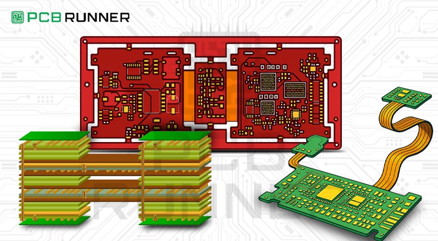
If you’ve ever opened up a remote, a toy, or even a laptop, you’ve probably seen a green or blue board with lots of tiny parts on it. That’s a circuit board. And all those little parts? They each have an essential job.

Understanding what these parts are and what they do can help you fix electronics, build your own devices, or simply understand how things work. If you ever work with a PCB board manufacturer or one of the top PCB manufacturers, this knowledge will make things easier.

Let’s look at the parts of a circuit board in a simple, straightforward way.

What Is a PCB?

PCB stands for Printed Circuit Board. It holds the electronic parts in one place and connects them with copper lines. These copper lines carry electricity between the parts, kind of like roads.

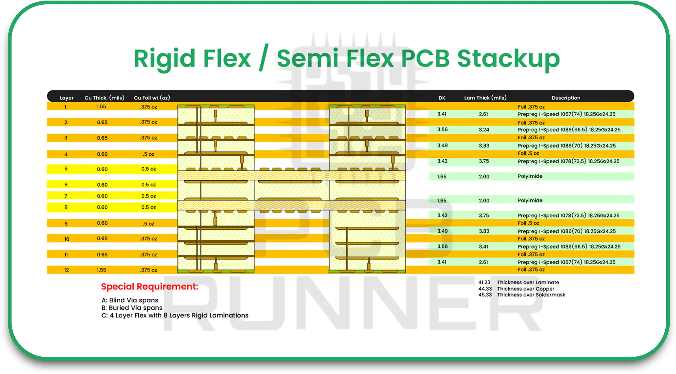
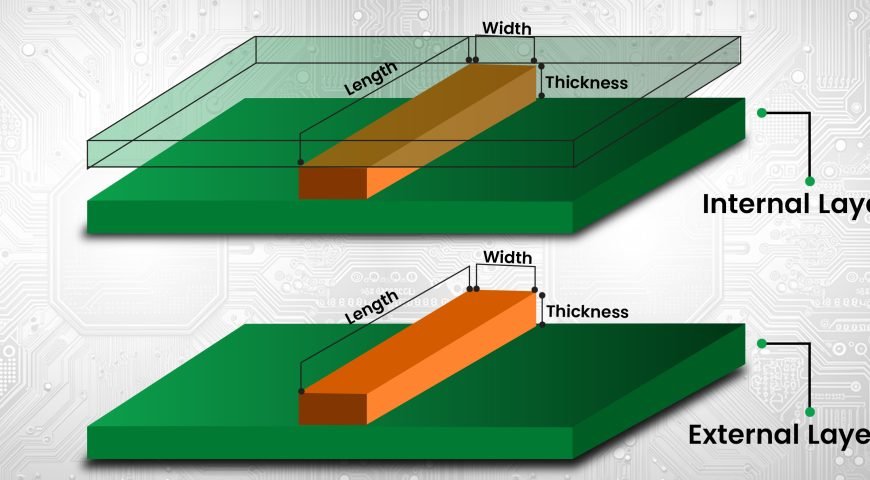
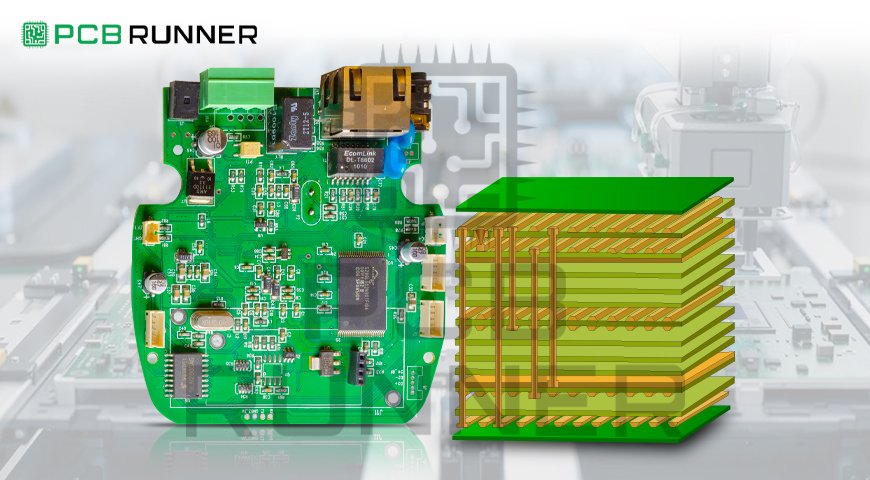
Some boards are simple, with just one layer. Others are complex, with many layers. These are called multilayer printed circuit boards. No matter the type, all PCBs have certain parts in common.

Why You Should Know the Parts

If you’re working with a PCB board manufacturer, identifying the parts correctly helps avoid mistakes. You can:

  • Explain your design better
  • Catch errors early
  • Save time during testing
  • Pick the right parts

You also won’t feel lost when looking at a board made by PCB manufacturers.

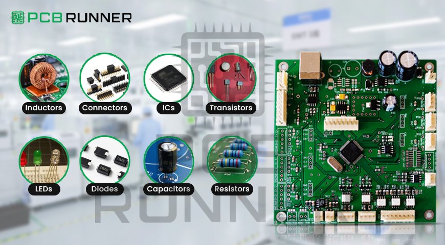
Key Electronic Circuit Board Components

Here are the basic parts you’ll see on most PCBs:
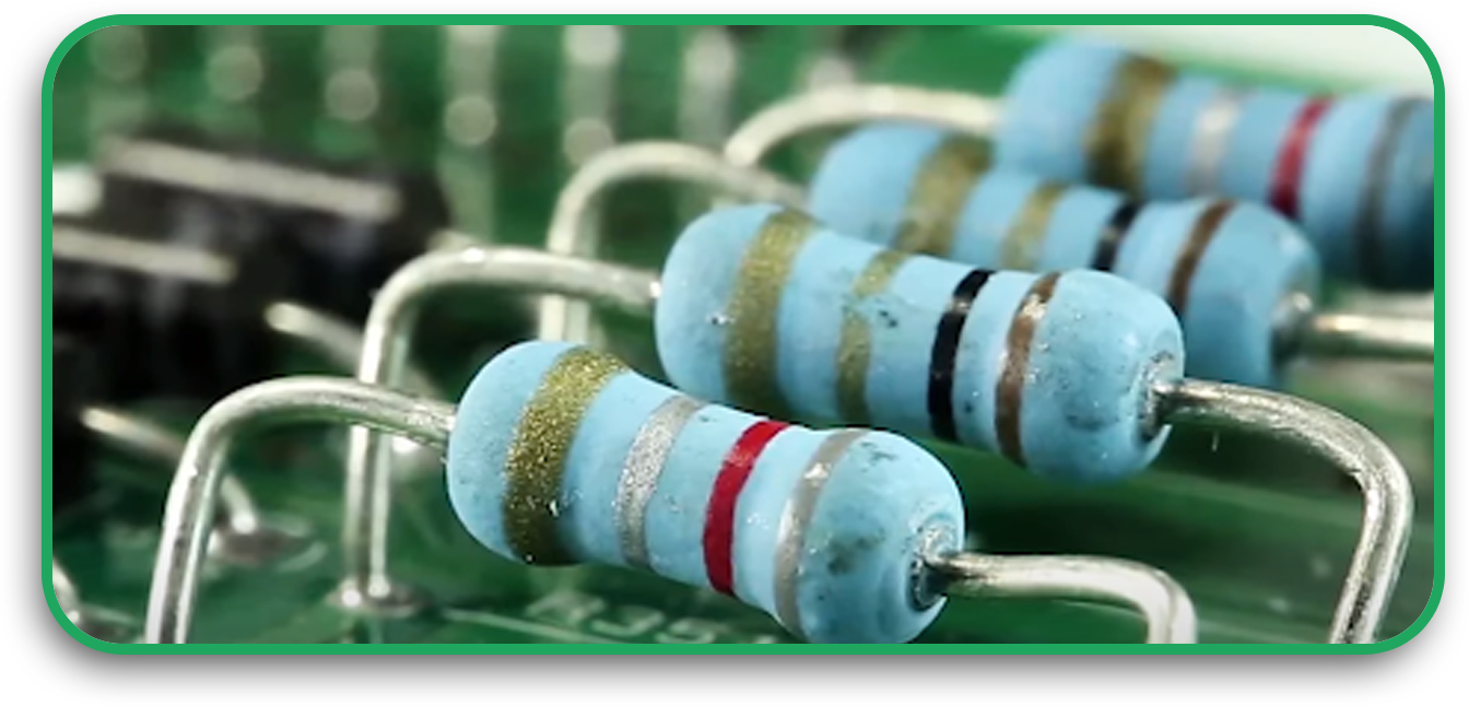
1. Resistors

  • Control the amount of electrical current
  • Look like tiny cylinders with coloured bands
  • Often labelled with an “R” followed by a number (like R1, R2)
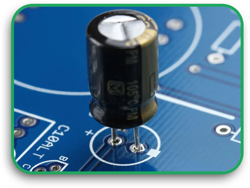
Resistors

2. Capacitors

  • Store and release energy quickly
  • Look like small barrels or discs
  • Labelled with a “C” and a number (C1, C2)
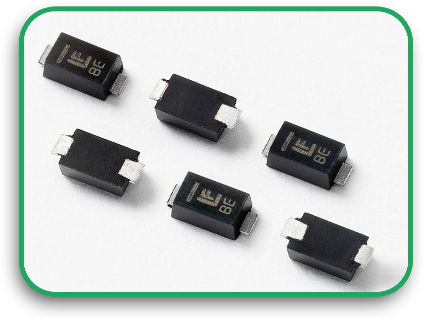
Capacitors

3. Diodes

  • Let electricity flow one way only
  • Look like small black cylinders with a silver stripe

Diodes

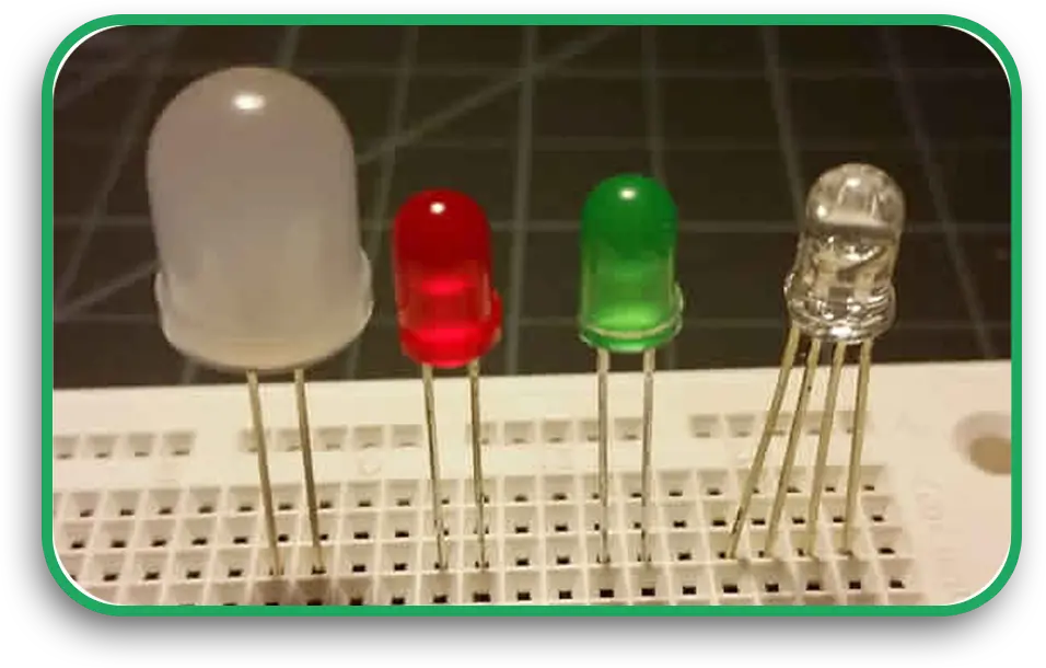
4. LEDs (Light Emitting Diodes)

  • Small lights that glow when current flows
  • Used as indicators (power on, charging, etc.)
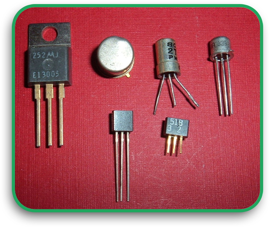
LEDs (Light Emitting Diodes)

5. Transistors

  • Control the flow of electricity like a switch
  • It can also increase (amplify) signals
  • Look like small black boxes with three legs

Transistors

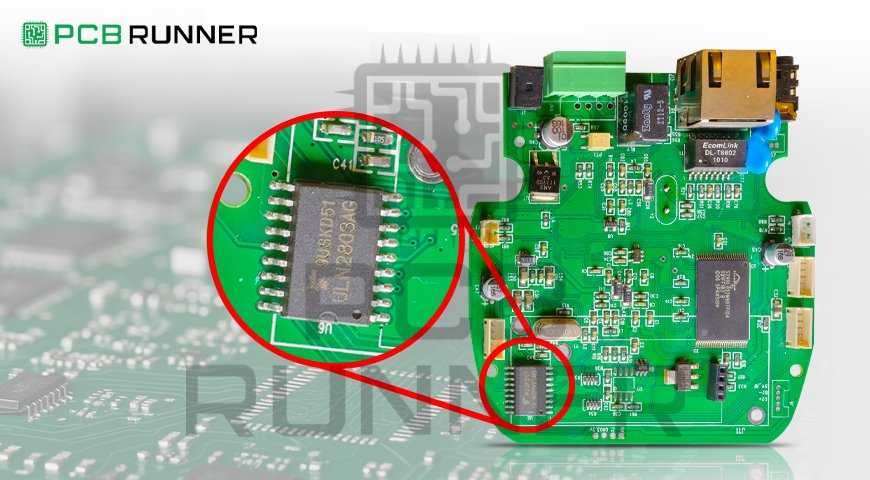
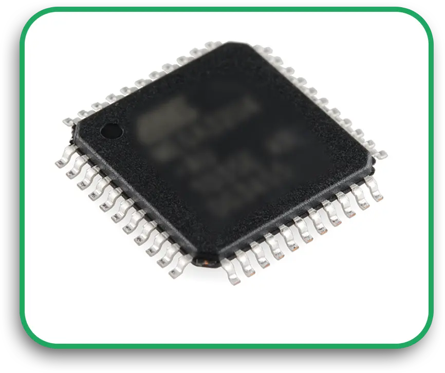
6. Integrated Circuits (ICs)

  • Also called chips or microchips
  • Do the real “thinking” or processing on the board
  • Look like black rectangles with many legs

Integrated Circuits (ICs)

7. Connectors

  • Allow the board to connect with power or other boards
  • Look like plastic blocks with metal holes or pins
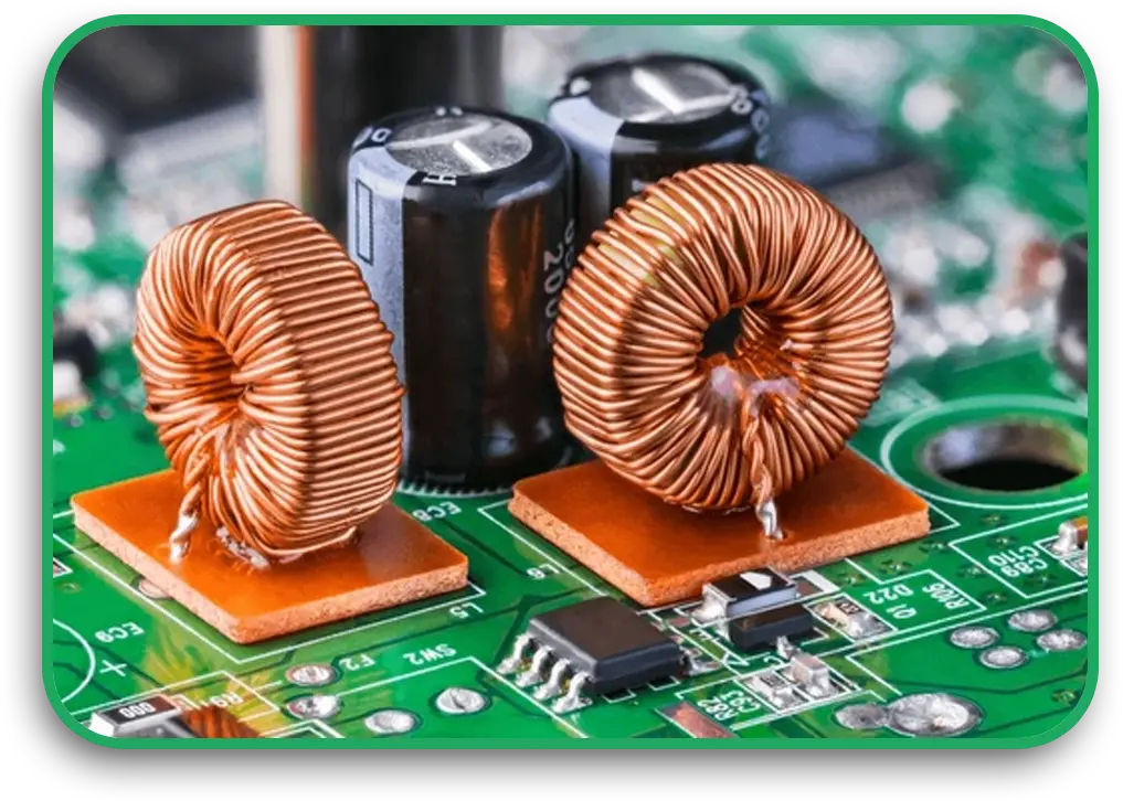
Connectors

8. Inductors

  • Store energy using a magnetic field
  • Look like wire coils or small blocks

Inductors

Learning to Identify Components

Want to learn component identification? Try these steps:

  • Look at the shape and number of legs
  • Find the label on the board (like R1, C3, U2)
  • Use a magnifying glass to check small parts
  • Search for part images online or in datasheets

If you’re using a board from a pcb board manufacturer, you can ask for a parts list. This list will tell you exactly what each piece is.

Understanding Circuit Board Parts

Each part plays a key role. If one fails, the whole board might stop working. That’s why pc board manufacturers take care when placing and testing each part.

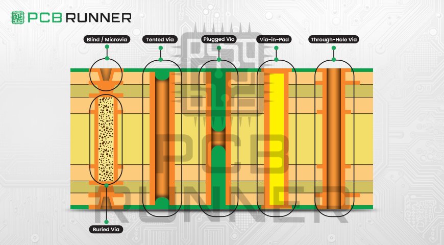
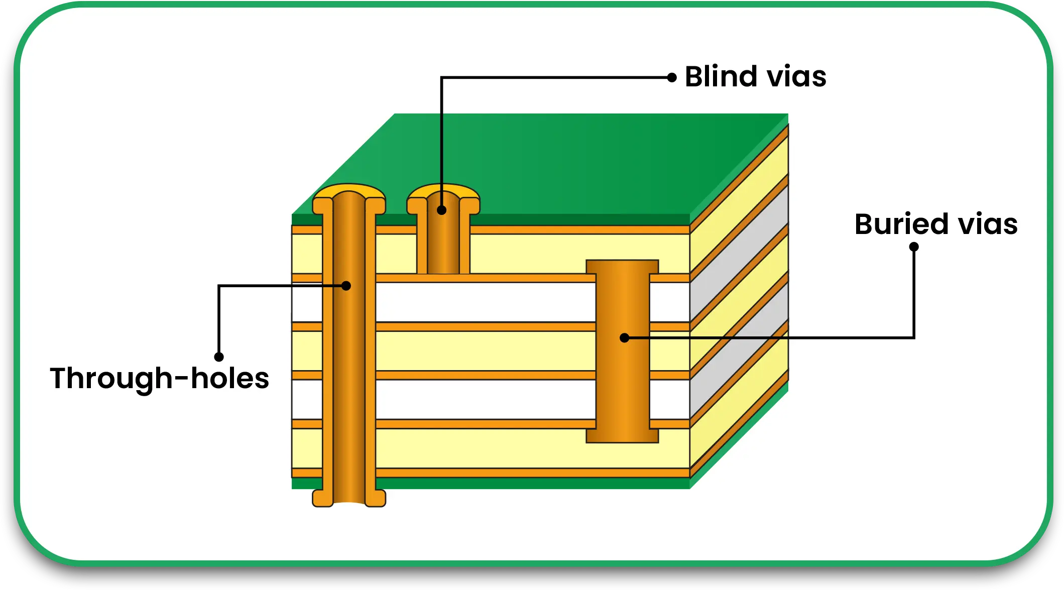
Even on a multilayer printed circuit board, the same basic parts are used. But the connections can run through different layers, which you can’t always see from the top.

If you’re fixing or designing boards, knowing where the parts are and what they do will help you spot problems fast.

Talking to PCB Manufacturers

When you work with pcb manufacturers, clear communication matters. If you know the parts by name, it’s easier to:

  • Choose replacements if a part is too expensive or slow to ship
  • Avoid putting parts in the wrong place
  • Test boards more accurately

Most PCB board manufacturers use files like a bill of materials (BOM) and layout diagrams. These show what parts go where.

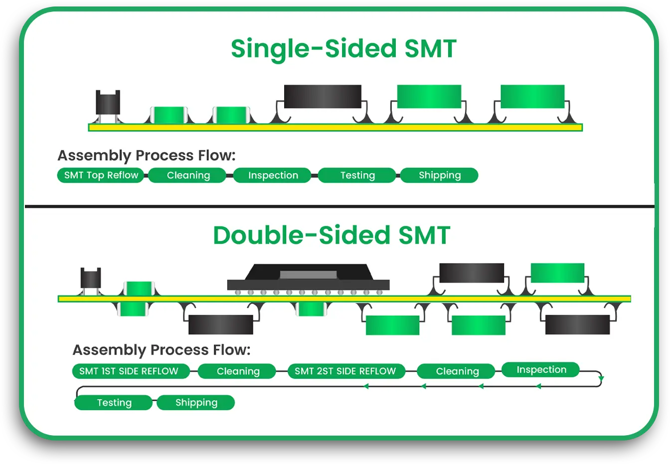
How PCB Components Are Assembled

Once the board is made, the parts are added. Some parts have legs that go through holes. These are called through-hole parts. Others sit flat on the surface. These are called surface-mount devices.

Most new boards use surface-mount parts. They’re smaller and cheaper. But they also need careful machines to place them right. That’s why choosing the right PCB manufacturers is essential.

When to Use Multilayer PCBs

Multilayer printed circuit boards are useful when your design is complex. For example:

  • Phones
  • Laptops
  • Medical tools

They let you fit more connections in a small space. But they can also make tracing problems harder.

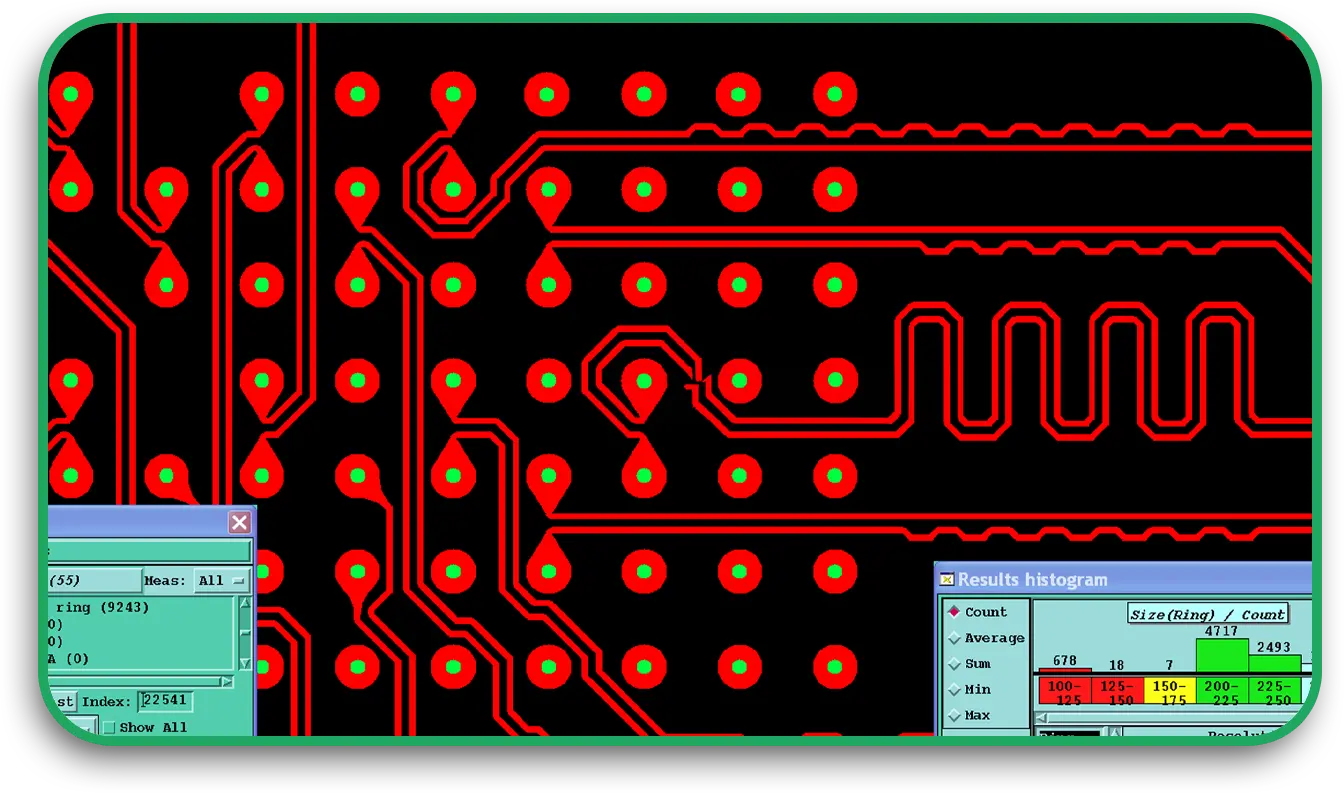
If you’re working with a PCB board manufacturer, ask them for a test report or an X-ray view of the inner layers.

Common Mistakes to Avoid

If you’re new to identifying circuit board parts, here are a few things to watch out for:

  • Mixing up resistors and diodes
  • Thinking all black chips are the same
  • Skipping part labels
  • Forgetting to check capacitor values

Even if a board looks simple, one missing part can stop everything. Always double-check.

Helpful Tools for Beginners

If you want to get better at component identification, try these:

  • A digital multimeter (to measure resistance and voltage)
  • A magnifier or microscope
  • Free online PCB viewers
  • Circuit board layout software

Some pc board manufacturers even provide test videos or 3D board previews. Ask for these if you’re ordering custom boards.

Final Thoughts

Knowing your electronic circuit board components gives you an edge. Whether you’re fixing a board, designing a new one, or working with a PCB board manufacturer, it helps to speak the same language.

Here’s a quick recap:

  • Learn the shapes and jobs of each part
  • Use part labels to guide your search
  • Practice with real boards or kits
  • Talk clearly with PCB manufacturers when designing or fixing

Start small, and don’t be afraid to ask questions. You’ll be surprised how fast you learn once you begin.

If you’re building your own design, choose experienced pc board manufacturers who understand your needs and can help you get the best results.

Need help with part sourcing or identifying parts on a damaged board? Reach out to a local PCB board manufacturer; many offer help for beginners.

Semi-Flex Circuit Boards

Semi-Flex Circuit Boards: The Future of Flexible Electronics

When most people think about electronics, they picture flat, rigid circuit boards inside phones, TVs, and computers. But did you know there’s a type of circuit board that can bend without breaking? It’s called a semi-flex circuit board, and it’s changing how we build and use electronic devices.

If you’re working with PCB circuit board manufacturers or designing a new product, it’s essential to understand this technology. Let’s explore what semi-flex PCBs are, how they work, and why they might be the right choice for your next project.

What Is a Semi-Flex Circuit Board?

A semi-flex circuit board is a special type of printed circuit board that can bend slightly in certain areas. These boards are made from a regular rigid material, like FR4, but with special processes that allow part of the board to flex without breaking.

They are not as flexible as full flex circuit boards, but they’re more bendable than standard rigid ones. That makes them perfect for tight spaces or products that need to move just a little.

Rigid flex stackup

Why Choose Semi-Flex Over Standard PCBs?

You might wonder: why not just use a regular flex and rigid PCB or a full rigid-flex circuit board?

Here’s why many engineers choose semi-flex PCBs:

  • Lower cost than full flex or rigid-flex boards
  • Simple to produce using regular materials
  • Ideal for tight spaces where a little bend is needed
  • Reliable for static bending (not repeated flexing)

If you don’t need your board to move constantly but still want flexibility for installation, this type of board works great.

How Are Semi-Flex PCBs Made?

Unlike full-flex circuit boards, semi-flex PCBs are made using regular FR4 material (a strong, heat-resistant type of fibreglass). A special milling or laser process thins out part of the board to allow it to bend.

These thinned sections are usually placed between two rigid areas. The flexible part connects them and bends when needed,like folding a hinge.

If you’re working with experienced pc board manufacturers, they’ll know how to build these correctly.

Where Are Semi-Flex Boards Used?

Semi-flex PCBs are used in devices where the board needs to bend once or a few times,usually during assembly.

Here are some common examples:

  • LED lighting systems
  • Medical devices
  • Car dashboards and control units
  • Industrial control panels
  • Consumer electronics like printers or cameras

In many cases, these boards replace costly cables or connectors. They also reduce space and improve reliability.


Semi-Flex vs. Flex and Rigid PCBs

Let’s compare a few features so you can pick the right board for your needs:

Feature Semi-Flex PCBs Flex Circuit Boards Rigid-Flex PCBs
Bending type Static (1–2 bends only) Dynamic (many bends) Static or dynamic
Cost Lower Higher Highest
Materials Modified rigid (FR4) Polyimide or flexible base Mix of rigid and flexible
Assembly process Easier and cheaper Needs special tools Complex and longer process
Space-saving Moderate Excellent Excellent

Benefits of Semi-Flex Boards

Working with reliable flex circuit board manufacturers or PCB board assembly companies gives you access to many benefits:

1. Space Saving

Bendable boards help fit electronics into small or oddly shaped devices without using extra wires.

2. Stronger Connections

They reduce the need for connectors and cables, which can come loose over time.

3. Lower Costs

Semi-flex boards are cheaper than fully flexible designs but still offer excellent performance.

4. Simpler Assembly

You can bend the board once and lock it in place. That makes the final product easier and faster to build.

Working With PCB Circuit Board Manufacturers

Not all PCB circuit board manufacturers have experience with semi-flex boards. Be sure to ask:

  • Have you built semi-flex boards before?
  • What’s the minimum bend radius you support?
  • Can you handle both PCB fabrication and PCB board assembly?

Choose a manufacturer that can guide you through the design process. They’ll help you avoid errors like placing parts in the bend area or using the wrong materials.

Design Tips for Semi-Flex PCBs

Here are a few practical tips when working with semi-flex:

  • Keep parts away from the flex area (at least 5mm)
  • Use curved traces in the end zone to prevent cracking.
  • Avoid vias in the flexible area.
  • Follow proper bend radius rules (ask your manufacturer)
  • Use stiffeners if needed for extra support.

Following these rules helps your board last longer and perform better.

Flexible Circuit Board Assembly: What to Expect

Whether you’re building a semi-flex, flex, or rigid-flex circuit board, the assembly process matters. During flex circuit board assembly, parts are usually placed on the rigid sections. The flexible part is kept clear to avoid stress or damage.

Good pc board manufacturers will have trained staff and machines that know how to handle flexible material. If they rush the process or skip steps, your board might not work correctly.

Ask your flex circuit board manufacturers how they handle storage, bending, and inspection.

Future of Semi-Flex in Electronics

As electronics get smaller and more complex, semi-flex boards are becoming more popular. They help make devices lighter, thinner, and more reliable.

New industries are now exploring semi-flex designs, including:

  • Wearable tech
  • Robotics
  • Smart home gadgets
  • Drones and electric vehicles

As electronic flex circuit board designs become easier to produce, you’ll see more companies switch to these bendable solutions.

Conclusion

If your design needs a little flexibility without the high price of full flex boards, semi-flex PCBs are a wise choice. They combine the strength of rigid boards with enough flex to fit into tight spaces. You save money, save space, and simplify assembly,all without sacrificing performance.

To get started, talk to trusted pcb circuit board manufacturers or flex circuit board manufacturers who understand your needs. Ask about bend radius, materials, and design tips. And don’t forget to plan for a safe, reliable PCB board assembly process.

By choosing the right board and the right partner, you can create better products,faster and wiser.


PCB Design

Optimising Your PCB Design for Via Current Handling: A Simple Guide

When building a printed circuit board (PCB), you may focus a lot on trace width or component layout. But have you ever thought about how much current your vias can carry? Vias are tiny holes with copper inside that connect different layers of a PCB. If they can’t handle the current, your board might overheat or even fail. That’s why knowing about current handling is important when designing any custom printed circuit board.

Whether you’re working with printed circuit board manufacturers or making a design on your own, learning how to handle current flow through vias can help you build a stronger, longer-lasting board.

What is a Via?

A via is a hole in the PCB filled or plated with copper. It lets current travel between different layers of the board. There are three main types:

  • Through-hole vias – go from top to bottom of the board
  • Blind vias – connect outer layer to inner layer
  • Buried vias – connect inner layers only

Each one helps the current move through the board. But not all vias can carry the same current carrying capacity.

Vias Types and Placement

Why Via Current Matters

Just like traces, vias have limits. If too much current flows through a via, it heats up. That heat can damage your board, melt the copper, or cause cracks over time. You need to make sure your via can carry the right amount of current for your circuit.

If you’re working with printed circuit board manufacturers, ask them to help calculate this during the design process.

Understanding PCB Current Carrying Capacity

Before we look at vias specifically, let’s understand the basics of PCB current carrying capacity. It’s the amount of current a copper trace or via can safely handle without overheating. This depends on a few things:

  • Width and thickness of the copper
  • Length of the trace or via
  • Temperature rise allowed
  • Whether it’s on the outer or inner layer

You can use a PCB current carrying capacity calculator to help figure this out. It gives you a rough idea based on your design choices.

How Via Size Affects Current

The via size is key. Larger diameter vias can carry more current. Smaller vias carry less. You also need to look at how thick the copper plating is inside the via.

A common rule: A via with 1 oz copper plating and 0.3 mm diameter can carry around 1 amp with safe temperature rise. But this is just a guideline. Always double-check with a PCB trace current carrying capacity calculator or your PCB board manufacturer.

Learnt About: How to Accurately Calculate PCB Trace Width

Ways to Improve Via Current Carrying Capacity

If your via needs to carry more current, here are some options:

1. Use Larger Vias

A bigger hole means more copper and less resistance. This can carry more current safely.

2. Use Multiple Vias

Instead of one large via, use several smaller ones in parallel. This spreads the current and reduces heat.

3. Increase Copper Plating

Ask your PCB manufacturer for heavier copper plating inside the via. This lets more current pass through.

4. Use Via-in-Pad

This method puts the via directly in the pad under a surface-mounted part. It saves space and helps with heat transfer too.

Real Example: Power Supply Board

Let’s say you’re making a power supply board. Some traces carry 5 amps or more. If the vias between layers are too small, they could fail fast.

In this case, you’d:

  • Use 3-4 vias in parallel
  • Make each via at least 0.5 mm wide
  • Ask for 2 oz copper plating

That helps spread the current and keeps the board safe. Your design works better, and you avoid future failures.

Choosing the Right Via for Your Design

When you plan your PCB, ask yourself:

  • How much current will pass through each via?
  • How many layers does my board have?
  • Is my current mostly DC or AC?
  • Do I need thermal relief?

These answers help you pick the right via size and layout.

If you’re not sure, your PCB circuit board manufacturer can help you figure it out. Always share your full design and ask for feedback.

Tools That Can Help You

Here are a few tools you can use during design:

  • PCB trace width calculator – helps with trace sizing
  • PCB current carrying capacity calculator – tells you how much current your trace or via can handle
  • Track width calculator – similar to trace width calculator, focused on track layout

These calculators let you test different values before sending your design for production.

Talking to Your Manufacturer

Always talk to your PCB board manufacturer early in the process. Share your:

  • Expected current levels
  • Temperature limits
  • Layout files
  • Layer count

The more info they have, the better they can guide you. Some PCB circuit board manufacturers offer free design review to check for weak spots in current handling.

Common Mistakes to Avoid

Here are some things to watch out for when designing for via current:

  • Using just one small via for high current
  • Forgetting to match the trace and via size
  • Ignoring temperature rise
  • Not testing your layout with a calculator

Fixing these mistakes early saves money and time later.

When to Use Custom Solutions

If you’re building something special like a custom printed circuit board, your current needs might be higher than usual. In this case, you may need:

  • Heavier copper boards (2 oz or more)
  • Filled vias (for better thermal and current performance)
  • Special via types like microvias

Talk to printed circuit board manufacturers that offer these services. Make sure they understand your design goals.

Final Thoughts

Vias are small, but they play a big role in your PCB’s performance. If they can’t carry enough current, your board might heat up, break down, or fail altogether. By choosing the right via size, using multiple vias, and checking with a PCB current carrying capacity calculator, you can keep your design safe and reliable.

Always put time into planning your via layout. Use tools. Talk to your pcb board manufacturer. And remember, every amp matters when you’re designing for long-term success.

Coating

Selective Coating Improves PCB Reliability: What You Need to Know

When you build electronic devices, one thing matters a lot—reliability. Your circuits must work in all kinds of environments. That’s where selective PCB coating comes in. It protects your printed circuit boards from dust, moisture, corrosion, and even vibration. Whether you’re working with home electronics or high-end machines, this type of protection helps your boards last longer and work better.

If you’re a PCB circuit board manufacturer or someone just learning how electronics work, understanding how selective coating boosts reliability can help you make smarter choices. Let’s break it down in a way that’s simple and easy to follow.

What is Selective Coating?

Selective coating means putting a protective layer only on certain parts of a PCB. Instead of covering the whole board, this process targets just the areas that need it. It’s different from full-board coating, where everything is covered—even parts that shouldn’t be.

The coating used is usually a conformal coating, which is a thin, protective film that “conforms” to the shape of the board and its components.

This makes it a perfect option for PCB circuit board manufacturers who want both precision and protection without wasting time or material.

Why Is Coating Needed?

Printed circuit boards face all kinds of dangers: water spills, dust, temperature changes, and even oil or chemicals in industrial spaces. If a circuit gets damaged, it could stop your whole device from working.

That’s why conformal coating for PCB is so essential. It keeps moisture out, stops corrosion, and makes the whole system more challenging.

In other words, you’re adding a thin shield to the brain of your device.

What Makes Selective Coating Better?

Here’s why selective PCB coating is often better than coating the entire board:

1. Protects Sensitive Areas Only

Some parts on a PCB shouldn’t be coated—like connectors or test points. Selective coating leaves these open while protecting everything else.

2. Saves Time and Money

You’re not wasting coating material or time covering the whole board. This is especially helpful for PC board manufacturers making lots of units.

3. Cleaner Application

Because the coating is applied only where needed, there’s less mess and less chance of coating mistakes.

Types of Coatings Used

Different coatings work better for different situations. Let’s look at some common types used by PCB circuit board manufacturers:

  • Acrylic Coating – Easy to apply and remove. Great for general protection.
  • Silicone Coating – Stands up to extreme heat and moisture. Used in cars, planes, or factories.
  • Urethane Coating – Strong against chemicals. Suitable for industrial use.
  • Epoxy Coating – Very tough but harder to remove. Used when strong protection is key.

Want the best conformal coating for PCB? That depends on what your board is being used for. A home device doesn’t need the same coating as a satellite system.

How the Coating is Applied

There are a few main ways conformal coating PCB can be applied:

1. Brushing

A person uses a brush to apply the coating by hand. Suitable for small jobs.

2. Spraying

This can be done with a spray can or automated system. Great for larger batches.

3. Dipping

The entire board is dipped in the coating. It covers everything unless masked beforehand.

4. Selective Coating Machines

These are machines that apply coating only to selected parts of the PCB using a robotic arm. This is what most modern pc board manufacturers use for accuracy and speed.

Why PCB Reliability Matters

When you think of a PCB, think of it like the brain of your device. If it fails, nothing else will work. That’s why improving PCB reliability is a top goal for every PCB circuit board manufacturer.

Imagine if your phone stopped working just because of a bit of moisture inside. That’s the kind of failure selective coating helps prevent. In harsh environments like aerospace, automotive, or medical devices, even a tiny flaw can be a big problem. Coating helps keep those flaws out.

What Should You Look for in a Coating Partner?

If you’re choosing a PCB manufacturer, ask these questions:

  • Do they offer selective coating?
  • Can they help you choose the best conformal coating for PCB based on your use case?
  • Do they have experience with custom-printed circuit boards in harsh environments?

The right partner will understand which areas of your board need protection and which don’t.

Key Benefits of Selective PCB Coating

Let’s quickly review what selective PCB coating offers:

  • Precision: Only coats areas that need it.
  • Efficiency: Saves material and reduces costs.
  • Protection: Shields from moisture, dust, and more.
  • Flexibility: Works with all types of PCBs, including flexible PCB boards.

Common Industries That Use It

Many industries count on conformal coating to keep their boards safe:

  • Automotive – for sensors and control units
  • Aerospace – for high-altitude conditions
  • Medical – for clean and reliable equipment
  • Consumer electronics – to keep your gadgets running longer

Everywhere you look, there’s a coated board behind the scenes keeping the system stable.

Real-Life Example: Why Selective Coating Matters

Let’s say you’re building a device that monitors temperature in a greenhouse. The air inside can get humid. Without protection, your board might corrode after a few weeks. But with a conformal coating, especially applied selectively, you can protect the key parts of your custom PCB without covering connectors that need to remain accessible.

That’s how a small layer of coating can prevent a big failure.

Final Thoughts

If you want your PCBs to work longer and better, selective PCB coating is worth considering. It gives your board the protection it needs without wasting time or money on full coverage. For PCB circuit board manufacturers and PC board manufacturers, it’s an easy way to boost reliability and reduce the risk of failure.

When done right, selective coating keeps your boards safe and your products strong—even in the harshest environments. It’s a smart step toward better electronics, no matter what you’re building.

Looking for a PCB partner? Choose one that offers high-quality coating services, understands your design, and helps you protect your investment with the right materials. Your circuits deserve it.

Surface Mount Technology

How Surface Mount Technology Changed PCB Design Forever

Change is the only constant in technology and electronics. There are many remarkable advancements in the design of printed circuit boards (PCBs); one of them is Surface Mount Technology (SMT). SMT changed the design and machines used to assemble and manufacture PCBs. Knowing how SMT operates and its effects on PCB design will help you understand the reason why it is known as the “game changer” of electronics.

Let us tell you more about what Surface Mount Technology (SMT) is, how it evolved PCB design and its advantages for PCB circuit board manufacturers and designers.

What is Surface Mount Technology (SMT)?

Before there was Surface Mount Technology (SMT), printed circuit boards (PCBs) used to be assembled using a method called through-hole technology. This method uses holes drilled into a board, where electronic components are placed and attached using solder on the opposing side. This technique works, but the large and heavy components required and assembling them was very tedious.

In contrast with SMT (Surface Mount Technology), through mounting techniques, the components are mounted onto the surface of the printed circuit board instead of routed through holes. The elements, referred to as Surface Mounted Devices (SMDs), are smaller in size and are meant to be placed on the top surface of the board. This enables the design of more compact and sophisticated assemblages, leading to adoption by almost all PCB board manufacturers.  

single sided smt and double sided

How SMT Changed PCB Design  

The impact of SMT on PCB design has been transformative, improving speed dramatically and efficiency and making space for more complex circuits. Below are just a few examples of how the landscape has changed:  

1. More powerful miniature devices  

SMT has a greater impact, which is the decrease in the size of components. Through-hole, components were big and bulky, which took a lot of space on the PCB, but with SMT, components are relatively more minor in size, which means more components can be fitted onto a single PCB. This not only led to the development of miniaturized and robust devices like smartphones, too, but also widened the scope of medical equipment.

For manufacturers of PCB circuits, this allows them to produce compact boards that are efficient and advanced in contemporary electronics technology. Also, they save space and material costs.

2. Faster and More Efficient Assembly Process

An improvement in one particular area of PCB assembly is SMT surface mounting technology, which is faster compared to previous techniques. Through-hole assembly, traditionally, every piece was painstakingly inserted into a hole and then soldered individually, which was a tedious and painstaking process.

SMT, on the other hand, utilizes automated machines that place the components on the surface of the PCB and not on the holes. Components are held in place by soldering them in a process called reflow soldering wherein the board is heated in a furnace, thus softening the solder paste and adhering the pieces in place. This approach diminishes the amount of manual work required, expedites the fabrication, and enhances the reliability of the results.

Because of the automation potential for PCB customization, custom printed circuit board suppliers experience increased productivity alongside reduced costs.

3. Better Performance and Reliability  

The small size of SMDs and their precise placement on the board automatically enhances the degree of reliability and performance. SMT components are more robust because they have fewer mechanical parts (like leads) that can be subject to wear and tear. Furthermore, the solder joints created by SMT surface mounting technology are more reliable because they tend to have better electrical connections, which strengthens the bond.  

Surface mount devices contribute to an overall decrease in the size and weight of the PCB, thus relieving the stress placed on the board and increasing its mechanical durability. This reduces the likelihood of suffering from failure due to extreme stress.  

4. Increased Component Density  

The use of SMT enables PCB designers to integrate more components onto the board as sufficed with higher component density. In through-hole designs, components were spaced further apart owing to their larger size. However, with SMT, components can be placed closer to one another, translating to more functionality available in a given space.  

This is extremely useful in the telecommunications industry, where high-density boards are needed. PCB circuit board manufacturers are able to design PCBs using SMT, incorporating more components while keeping the size manageable in view of the powerful and compact devices designed.

5. Cost Efficiency  

Smaller size and faster assembly add cost savings due to the use of SMT surface mounting technology. PCB board manufacturers can accomplish more in less time, resulting in decreased labour and material expenses. In addition, smaller components are usually less expensive than their through-hole counterparts, lowering costs even more.  

Moreover, the use of automated pick-and-place machines means the manufacturer can reduce the use of human hand work in the production process, enhancing resource efficiency and lowering costs. This results in decreased overhead for the production of each board.  

6. Design Flexibility and Innovation  

The invention of SMT has permitted greater flexibility in design. Engineers can custom print circuit boards without as many restrictions as before. The availability of smaller and densely packed components allows for innovative printed circuit board designs which are not feasible with through-hole technology.  

This flexibility enables the production of a broader range of products, from consumer electronics to automotive systems. For PCB board manufacturers, this flexibility means greater challenging designs that can be tailored to client needs.

7. Enhanced Testing and Inspection Capabilities

The Innovations made in Surface Mount Technology (SMT) has also improved the methods used in Testing and inspection of PCBs. Automated Optical Inspection (AOI) systems can effectively and rapidly find errors in surface mount devices. This guarantees that only good and defectless boards come to the higher stage of production.

Moreover, the Standardized geometry and small size of SMDs also facilitate inspection during the production process. This improves yield and decreases the number of defective boards, which benefits PC board manufacturers in the form of savings and increased customer satisfaction.

Key Components of SMT

To analyze the implications of SMT, it is essential to learn the fundamental constituents of SMT surface mounting technology first:

Surface Mount Devices (SMDs): These are the Electronic components that are mounted on the surface of the PCB. Resistors, capacitors, diodes and integrated circuits (ICs) are some common examples of SMDs.

Reflow Soldering: This refers to the process of melting solder and affixing the SMDs onto the board by heating the PCB.

Pick and place machines: These are mechanical devices that position the SMDs on the board in advance of the reflow soldering phase.

Conclusion

Surface Mount Technology (SMT) is a game-changer because it enhances the efficiency of PCB design, reduces costs, improves manufacturing precision, and enables the development of smaller and more powerful devices. Physically Smaller parts, quicker assembly, and better component placement enables the electronics design innovation due to SMT.

For manufacturers of PCB circuit boards, the adoption of SMT surface mounting technology results in more advanced, cost-effective, high-performance PCBs. SMT is now central in fulfilling the requirements of modern technology design for consumer electronics and industrial devices due to the compact, reliable, and efficient design it enables.

SMT will continue to serve as the backbone for advancements in custom printed circuit boards across myriad applications in future and will help professional designers address the challenges of tomorrow.

PCB Trace

How to Accurately Calculate PCB Trace Width

Printed Circuit Boards (PCBs) are the backbone of nearly all modern electronic devices. One of the key components of a PCB is its traces, which are the electrical paths that connect the various components of the board. These traces are responsible for carrying current and signals between components, so it’s crucial to ensure they are sized correctly for the board to function properly.

One of the most essential factors in PCB trace design is the trace width. The trace width refers to the physical width of the copper traces on a PCB. This width must be carefully calculated to ensure that the traces can carry the required current without overheating or becoming too weak to function correctly.

In this blog, we will walk you through the steps of calculating the correct PCB trace width, as well as how to use trace width calculators to make the job easier.

Why Trace Width Matters?

Before we dive into the details of how to calculate trace width, it’s essential to understand why it matters in the first place. PCB traces are made from copper, which is a good conductor of electricity. However, the width of the trace plays a crucial role in determining how much current the trace can safely carry.

If the trace is too narrow, it may overheat due to high current flow, leading to a failure of the PCB. On the other hand, if the trace is too broad, it may take up too much space on the PCB, leaving less room for other components or traces. Therefore, calculating the correct trace width is essential for both safety and efficiency.

Factors That Affect PCB Trace Width

When calculating PCB trace width, there are several factors you need to take into consideration:

  1. Current Carrying Capacity: This refers to how much current the trace needs to carry. Higher currents require wider traces to prevent overheating.
  2. Copper Thickness: The thickness of the copper used for the PCB will impact the trace width. Thicker copper can handle more current so that the trace width can be narrower.
  3. Temperature Rise: The temperature rise refers to how much the trace temperature increases due to the current. You want to keep the temperature rise within safe limits, so you need to adjust the trace width accordingly.
  4. PCB Manufacturer Specifications: Different PCB circuit board manufacturers may have different guidelines or limitations on trace width and spacing. Always check with your PCB board manufacturer for their specifications before finalizing your design.

How to Calculate PCB Trace Width

Now that we know why trace width is essential, let’s go over how to calculate the width of the traces for your PCB accurately. The formula for calculating trace width is based on the amount of current the trace needs to carry, the copper thickness, and the allowable temperature rise. Here’s a simple formula:

W=Ik×(Tr)0.5W = \frac{I}{k \times (T_r)^{0.5}}W=k×(Tr​)0.5I​

Where:

  • W = Trace width (in mils or mm)
  • I = Current (in amperes)
  • k = A constant that depends on the copper thickness (typically between 0.5 and 1.2)
  • T_r = Temperature rise (in Celsius)

While this formula gives you an idea of how to calculate trace width manually, it can be complex and time-consuming. Thankfully, there are tools available to make this process easier.

pcb trace calculator

Using a PCB Trace Width Calculator

Rather than calculating trace width manually, many PCB board assembly companies and PCB circuit board manufacturers provide online trace width calculators to simplify the process. These calculators allow you to input key information, such as:

  • Current (in amperes)
  • Copper thickness (in oz/ft²)
  • Temperature rise
  • Units (mils or mm)

Once you input these values, the calculator will output the optimal trace width for your PCB design. Many online calculators are free to use and can help you save time and reduce the likelihood of errors.

There are several popular PCB trace width calculators available, such as:

  • IPC-2221 Trace Width Calculator: This calculator follows the standards set by the IPC (Institute for Printed Circuits) and provides a reliable way to determine trace width.
  • Online Trace Width Calculator by Advanced Circuits: This free tool allows you to quickly determine the trace width based on the current and other parameters.
  • EasyEDA Trace Width Calculator: This tool is integrated with the EasyEDA design software, making it convenient for designers working with the EasyEDA platform.

By using these tools, you can quickly and accurately calculate the track width required for your PCB design without the need for complex formulas or manual calculations.

The Role of PCB Design Software

When designing a PCB, many PCB circuit board manufacturers and engineers rely on specialized printed circuit board design software to create the layout. These software tools often come with built-in features that can automatically calculate trace width, saving even more time and reducing the risk of human error.

Some PCB design tools that include trace width calculation features are:

  • Altium Designer: One of the most widely used design tools, Altium Designer has an integrated trace width calculator that can help designers select the right trace width based on their design requirements.
  • KiCad: A free and open-source PCB design tool, KiCad offers features to help you determine trace width based on current and copper thickness.
  • Autodesk Eagle: Known for its user-friendly interface, Eagle allows designers to input trace width settings. It will provide feedback during the design process to ensure that the trace width is appropriate.

These tools often integrate directly with PCB fabrication processes, allowing manufacturers to transition from design to production without errors easily.

What Happens If You Get the Trace Width Wrong?

Incorrect trace width can lead to various problems in your PCB. If the trace width is too narrow, the trace may overheat, leading to potential failure. If the trace width is too wide, you may waste valuable PCB space, increasing the size and cost of your design.

In some cases, overly narrow traces can cause a PCB failure during operation. On the other hand, wide traces may contribute to larger board sizes or unnecessary cost increases. That’s why accurate trace width calculation is essential for maintaining reliability and performance.

Conclusion

Calculating the correct PCB trace width is crucial for ensuring the success of your PCB design. By understanding the factors that affect trace width, such as current carrying capacity, copper thickness, and temperature rise, you can make informed decisions about your design. Using trace width calculators and PCB design software will help you save time and reduce errors in your design. Whether you’re a PCB board manufacturer, engineer, or DIY designer, taking the time to calculate trace width accurately will ensure that your PCB works reliably and efficiently.

Make sure to check with your PCB board manufacturer for any specific design guidelines, and always test your designs thoroughly before moving to production. With the right tools and knowledge, you can create high-quality, reliable PCBs that meet your specifications.


Printed Circuit Board Manufacturer

The Best Checklist for Choosing a Printed Circuit Board Manufacturer

Choosing the right PCB manufacturer can make or break your project. If you want to avoid delays, low-quality boards, or costly mistakes, start with the right partner. This checklist will guide you step by step, whether you need simple or flexible PCB boards.

Why Your Choice of Manufacturer Matters

A strong design means nothing if the board fails in real use. Weak soldering, poor materials, or missing inspections can lead to returns or unsafe products. That’s why your choice of a PCB circuit board manufacturer is a big deal. It’s about more than just price.

Start with Certifications

Look for certifications. Good PCB manufacturers follow global safety and quality rules. These show they have systems in place to make reliable boards.

  • ISO 9001: Basic quality management
  • UL Certification: For safety checks
  • IPC Standards: For board building and inspection

If your project needs high trust, like in medical or car tech, extra certifications matter too.

Cirtifications_

Ask About Board Types

Not all manufacturers offer the same boards. Make sure they can build what you need:

  • Single or double-layer boards
  • Multilayer printed circuit boards
  • Flexible PCB boards
  • Rigid-flex boards
  • High-density interconnect boards

You want someone who’s done this before. Ask for real examples.

What Materials Do They Use?

The material of PCB affects how well it works. Some materials handle heat better. Others are great for signal flow. Ask about the base they use:

  • FR4: Common and cost-friendly
  • Polyimide: Great for flexible PCB board needs
  • Rogers: Best for high-frequency signals

Check how they test and store these materials too.

materials

Do They Check Your Design Files?

Even if you use great printed circuit board design software, errors can slip in. Good pc board manufacturers will help you catch mistakes early.

  • They should review Gerber files
  • Offer DFM (Design for Manufacturing) help
  • Suggest small tweaks that cut cost or boost quality

This saves time and avoids waste.

dfm

Can They Meet Your Timeline?

Some projects need speed. Others need large volumes. The best PCB manufacturers will offer both.

  • Ask about standard and rush jobs
  • What’s the lead time for 10 vs. 10,000 boards?
  • Can they scale up later?

Make sure faster doesn’t mean lower quality.

Order Size Flexibility

Not every project needs a large batch. Some start with a few boards. Good pcbs-sales partners understand this.

  • Do they offer low-volume builds?
  • Can they ramp up if demand grows?
  • Will they adjust prices as volume changes?

This flexibility helps you grow without stress.

Testing and Inspection

Every board should be checked before it leaves the factory. Ask what PCB inspection methods they use:

  • AOI (Automatic Optical Inspection)
  • X-ray (for hidden solder joints)
  • Electrical testing (to check for shorts or gaps)

They should also follow clear quality steps like IPC-A-600. This is the heart of PCB quality assurance.

Assembly Services

Some pc board manufacturers also build your board with all parts included. That means you get finished boards, not just bare ones.

This saves time and lowers the risk of errors.

Communication and Support

You want a team that replies fast, clearly, and with helpful answers. Poor support now means worse problems later.

  • Do they respond in 24 hours?
  • Can they explain processes without jargon?
  • Is there one contact person for your project?

Clear answers build trust.

Company Reputation

Check reviews or ask for references. You can also search online forums for feedback.

  • How many years in business?
  • What types of industries do they serve?
  • Do they offer real success stories or client names?

Past performance often shows future results.

Understand How a PCB Is Made

Even if you’re not the engineer, you should understand how a PCB is manufactured:

  1. Review design files
  2. Print the layout on copper layers
  3. Etch away unused copper
  4. Drill holes for connections
  5. Add copper plating to holes
  6. Apply solder mask and labels
  7. Test and inspect each board

Knowing this helps you ask smarter questions.

Checklist Summary

Use this final list to compare PCB circuit board manufacturers:

  • Are they certified and safe?
  • Do they offer the board you need?
  • Do they use strong, tested materials?
  • Will they review and improve your design?
  • Can they meet your timing needs?
  • Do they accept your order size?
  • Do they test boards fully?
  • Can they also assemble the board?
  • Do they reply clearly and quickly?
  • Do they have strong reviews?

Bonus Tips

  • Always ask for a sample before a big order.
  • Get a written quote with lead time and terms.
  • If it sounds too cheap, ask why.

Final Thoughts

Picking the right manufacturer is more than a quick search. It’s a key decision. The right choice gives you strong, reliable boards that work the first time. It also helps you grow your product without delays or poor quality.

Use this checklist to compare suppliers. Ask clear questions. And trust your gut if something feels off. A good partner will welcome your questions and walk you through each step.

That’s how you build success from the ground up—starting with your circuit board.

PCB Panel Sizes

A Complete Guide to Standard PCB Panel Sizes and Board Dimensions

Want to save money and reduce errors during manufacturing? Start by getting your PCB panel size right. Standard PCB panel sizes help reduce waste, lower fabrication costs, and simplify the production process. Whether you are working with simple boards or high-density interconnect designs, knowing your PCB board dimensions and layout can make all the difference.

IThis blog will discuss standard PCB panel sizes, how to choose the right one for your project, and how this impacts your final cost and board quality.

Why PCB Panel Sizes Matter

When you send your design to a PCB circuit board manufacturer, one of the first things they check is your panel size. A panel is a large sheet that holds multiple PCBs. These panels are then processed as a whole before being separated into individual boards.

Using a standard PCB panel size means your design fits the manufacturing equipment without custom changes. This keeps production smooth, lowers your cost, and avoids waste.

Key Benefits:

  • Maximises board yield per panel
  • Reduces setup and tooling costs
  • Improves material usage
  • Helps meet tight deadlines with less back-and-forth

What Is the Standard PCB Panel Size?

Most PC board manufacturers use the 18 x 24-inch panel as a common size. However, not all of this space is usable. Part of the panel is reserved for tooling holes, test coupons, and routing spacing.

The usable area is usually around 16 x 22 inches, depending on the manufacturer and how they handle margins.

Panel Size Usable Area Notes
18” x 24” ~16” x 22” Most commonly used
12” x 18” ~10” x 16” Good for small boards
21” x 24” ~19” x 22” For large-volume boards

Choosing the right panel size helps balance cost and efficiency. A good pcb fabrication shop will help you plan how many boards you can fit into one panel, called the panelization process.

PCB Panel Sizes


Understanding PCB Board Dimensions

Before you consider panel size, you need to know your individual board size. Most boards are between 2 x 2 inches and 10 x 10 inches, but there’s no strict rule. It all depends on your application and the available space inside the product housing.

Still, there are some points to keep in mind:

  • Boards wider than 12 inches may require custom tooling
  • Tiny boards (<1 inch) often need to be grouped in large arrays.
  • Boards with high component density, like high-density interconnect (HDI) PCBs, might require more panel spacing.

How Board Size Affects Cost

Your board size and how many boards you can fit in a panel affect your final cost. Here’s how:

  • Smaller boards use less material but can be wasteful if poorly penalised.
  • Larger boards use more material but may lower the cost per component due to fewer interconnects.
  • Odd shapes or non-rectangular boards reduce panel efficiency.

That’s why top PCB circuit board manufacturers work closely with you to get the best yield. They use advanced tools and software to calculate the best fit per panel.

Panelization Basics

Panelization is the process of placing multiple copies of your board into one panel. The goal is to make the best use of space, simplify assembly, and reduce waste.

Here’s how you typically penalise boards:

  1. Determine individual board dimensions
  2. Add spacing between boards (usually 0.1 to 0.2 inches)
  3. Add tooling holes and fiducials.
  4. Add breakaway tabs or v-grooves to separate boards later.

Your PCB board dimensions should allow multiple boards to fit neatly inside the usable area of the standard PCB panel size. This helps keep the manufacturing cost-effective and straightforward.

Tips for Efficient Panel Design

To make sure you get the most out of your panel, follow these design tips:

1. Stick to standard dimensions

Stick to standard panel sizes unless your project requires something special. Custom sizes can slow down production and increase costs.

2. Leave enough spacing

Space between boards is needed for routing, panelling, and handling. Too little space increases the risk of damage.

3. Optimise board orientation

Some boards can be rotated to fit more units in a panel. Your PCB fabrication partner can help with this layout trick.

4. Group small boards

If your boards are tiny, consider grouping them into an array to speed up assembly and testing.

What About High-Density Interconnect (HDI) PCBs?

High-density interconnect (HDI) boards are smaller and more complex. To save space, they use micro vias, thinner traces, and more layers. While this means better performance, it also means tighter controls on board dimensions and panel layout.

Some points to consider:

  • HDI boards may need tighter spacing rules
  • Panels need more precise alignment.
  • Standard panel sizes are still used, but yield may be lower.

Work with an experienced HDI PCB manufacturer who understands how to handle HDI designs during panelization and fabrication.

How PCB Manufacturers Handle Custom Boards

Sometimes, your board shape or size doesn’t fit the standard format. That’s okay. Custom boards are common. However, they take more planning. Most pc board manufacturers will suggest:

  • Using a custom panel size
  • Including extra material for support
  • Designing break-off tabs carefully to avoid damage

When working with custom printed circuit board layouts, early communication with your PCB fabrication shop can help avoid problems later.

What You Should Ask Your Manufacturer

When choosing from PCB circuit board manufacturers, make sure to ask:

  • What panel sizes do you support?
  • What is your usable area on the panel?
  • How do you handle odd-shaped boards?
  • Can you help with panelisation planning?
  • What are your limits for high-density interconnect boards?

These questions will help you make the right choice and avoid delays.

Final Thoughts

Choosing the correct PCB board dimensions and panel size might not sound exciting, but it’s a key part of reliable and cost-effective production. Whether you’re making standard boards or working with high-density interconnect, good planning at this stage will save time and money later.

By working with trusted PC board manufacturers and using smart design practices, you can get better-quality boards, faster turnaround, and lower costs.

Key Takeaways

  • The most common standard PCB panel size is 18 x 24 inches.
  • The usable area is less than the whole panel due to spacing and tooling holes.
  • Good penalisation reduces waste and cost.
  • Work with your PCB fabrication partner early to plan the layout.
  • Custom boards may need extra care but are manageable.
  • HDI boards require tight spacing and experienced handling

FAQs

Q: What is the typical spacing between boards in a panel?
A: Usually 0.1 to 0.2 inches, but it depends on routing and depaneling method.

Q: Can I use non-rectangular board shapes?
A: Yes, but they reduce panel efficiency and increase cost. Grouping or rotating may help.

Q: Are there special rules for HDI PCBs in panels?
A: Yes. HDI boards use tighter tolerances and may need extra alignment during fabrication.

Q: Who should plan the panel layout?
A: Your PCB circuit board manufacturer often handles this, but it’s best to collaborate early.

Q: How many boards fit on one panel?
A: It depends on the PCB board dimensions and how well they fit the usable area. A manufacturer can calculate this for you.

PCB Functional Testing

The Importance of PCB Functional Testing and Quality Assurance for Reliability

When you build or buy a printed circuit board (PCB), you want it to work the first time. Whether it is going into a phone, a car, or an industrial machine, your PCB must be reliable. This is why PCB functional testing and quality assurance matter so much. If something goes wrong after the board is assembled, fixing it later can cost time and money. Even worse, a bad board in a critical system can lead to more significant problems. Let us look at why testing and quality checks are a must and how they work.

Why Reliability in PCBs Matters?

Your PCB is like the heart of your device. If it fails, the whole system can stop working. For you as a user, this means frustration. For businesses, it can mean returns, repairs, and unhappy customers. Poor reliability can even damage a brand’s name. That is why reliable boards are a top priority for PCB manufacturers.

What Is PCB Functional Testing

PCB functional testing is the process of checking whether your board does what it is supposed to do. After the board is built and all the parts are in place, it is tested using tools that simulate how it will work in real life. It is like a final exam for your board.

Here are some things tested:

  • Power supply lines
  • Signal lines
  • Response to inputs
  • Output levels

If anything does not work as expected, it is flagged and reviewed.

What Does Quality Assurance Mean in PCBs?

Quality assurance (QA) is a set of steps taken during PCB design and assembly to ensure the end product works as expected. It starts even before the board is built. QA helps catch problems early so you don’t waste money building boards that don’t work.

Some QA tasks include:

  • Checking the design using printed circuit board design software
  • Making sure parts are placed correctly
  • Testing how well solder joints are made
  • Final inspection of each board before it leaves the factory

This is where trusted PCB manufacturers make a big difference.

Different Types of PCB Testing

There are many ways to test a PCB. Each one looks at something different. You can think of them as layers of checks, each catching something the other might miss. Here are the most common PCB inspection methods:

1. Visual Inspection

This is the first step. A technician looks at the board with the naked eye or a magnifier. They check if parts are aligned and if there are any apparent problems, such as missing parts or extra solder.

2. Automated Optical Inspection (AOI)

This uses cameras to scan the board and compare what it sees to the design files. If there is a mismatch, the board is marked for review. AOI is fast and can spot tiny problems humans might miss.

3. X-Ray Inspection

If your board has parts hidden under chips, like with flex and rigid PCB designs, X-rays help see through layers. They can also check for hidden solder issues or broken connections.

4. In-Circuit Testing (ICT)

This test checks each part on the board. It can test resistors, capacitors, and chips to see if they are working and if each part is in the right place.

5. PCB Functional Testing

This final test checks whether your board behaves as it should. It is usually done with a test fixture made for your board. The fixture connects to the board and runs real-world tests on it.

Quality Assurance Starts with Design

The first step in quality assurance PCB work starts with good design. If your design has mistakes, no amount of testing can save it. That is why printed circuit board design software plays such a significant role. These tools can catch many issues early, such as short circuits, wrong part placements, or spacing problems.

Once the design is checked and approved, the fabrication and assembly process begins. Multistep QA processes are in place throughout:

  • Clean rooms to keep dust out
  • Machines that place parts with high accuracy
  • Heating systems for perfect solder joints
  • Ongoing spot checks during the circuit board assembly process

Flex and Rigid PCB Testing

Flex PCBs can bend, while rigid ones cannot. Some boards combine both. Testing these requires special care. If not made right, flex boards may fail after bending. Testing includes stress tests to see how many times the board can bend before it breaks. This is key for products like wearables and foldable electronics.

Why PCB Reliability Testing Is Crucial

Even if a board passes early tests, it may still fail later. That is why PCB reliability testing checks how your board holds up over time. These tests include:

  • Heat tests (does it work in hot conditions?)
  • Cold tests (can it handle freezing temperatures?)
  • Vibration tests (will it stay together in a moving car?)
  • Humidity tests (does moisture cause shorts or corrosion?)

These tests help prove that the board will work for years, not just for a few hours.

Choosing the Right Manufacturer

Not all PCB manufacturers are the same. You want a company that takes quality seriously. Look for those that:

  • Use up-to-date printed circuit board design software
  • Have strong QA teams
  • Offer both flex and rigid PCB production
  • Have good reviews and strong client feedback

Ask if they do full PCB functional testing and how they handle failures during testing. Good suppliers will explain their inspection and testing process in detail.

What You Can Do as a Customer

You do not need to test your boards yourself, but there are things you can do to help the process go smoothly:

  • Share clean design files
  • Include test points in your layout
  • Choose a PCB board manufacturer like PCB Runner with proven QA experience

Your choices can help catch problems early and avoid extra costs later.

Final Thoughts

Reliable boards do not happen by accident. They are the result of careful design, quality materials, good assembly, and vigorous testing. When you work with printed circuit board manufacturers who understand the importance of quality assurance PCB methods, you get better results. From the tools used in printed circuit board design software to the final PCB functional testing and reliability checks, every step matters. Whether you are building a single board or thousands, never skip testing. Your users, your product, and your peace of mind depend on it.

Multilayer Printed Circuit Boards

Multilayer Printed Circuit Boards: Modern Technology with Multilayer PCBs

If you are working with modern electronics, you’ve likely come across multilayer printed circuit boards. These boards are more than just a bunch of copper layers stacked together. They are at the heart of your smartphone, laptop, medical device, and even your car. In this post, we will explore how multilayer PCBs help you get more out of your design, why they matter, and what you need to know when choosing a reliable PCB circuit board manufacturer.

What Is a Multilayer Printed Circuit Board?

A multilayer printed circuit board has more than two layers of conductive copper stacked with insulating layers in between. This setup allows you to route more signals and power connections in a compact space.

A simple board might have two layers, one on the top and one on the bottom. But modern systems need more. A multilayer PCB board might have four, six, eight, or even over twenty layers.

This type of board offers better performance, a smaller size, and stronger connections. That’s why it is so common in smartphones, routers, tablets, and advanced control systems.

Why Use a Multilayer PCB Board?

If your device is doing a lot of tasks at once or if you want it to be compact, a multilayer PCB design is often the best answer. Here’s why:

    • Space Saving: More layers mean you can route signals in tighter spaces.
    • Better Signal Quality: Having separate ground and power planes helps reduce noise.
    • Strong Performance: These boards can handle high-speed signals with ease.
    • Less Weight: You can build smaller and lighter systems.

When you choose the right PCB circuit board manufacturer, you ensure these benefits come to life without the risk of faulty builds.

Key Materials in Multilayer PCB Fabrication

A good multilayer board starts with the right materials. You’ll often see boards made of FR-4, a strong and heat-resistant type of fibreglass. For high-performance or high-frequency work, you may need other materials like polyimide or PTFE.

The core, a rigid layer of fibreglass, is in the centre of a multilayer PCB board. It is laminated with prepreg (pre-impregnated) layers, then pressed and heated to form one strong piece.

Choosing the right materials during multilayer PCB fabrication is critical to ensure your board can handle both mechanical and thermal stress. Your PCB circuit board manufacturer will help guide you based on your design and budget.

Multilayer PCB Design Tips

Designing a multilayer board isn’t just about stacking layers. You need a clear plan. Here are some practical tips to follow:

    1. Plan Your Stack-Up Early: Decide how many signal, power, and ground layers you need.
    2. Keep Signal Paths Short: Shorter paths reduce delay and signal loss.
    3. Use Ground Planes Wisely: Solid ground planes reduce noise and improve return paths.
    4. Avoid Crosstalk: Keep high-speed lines apart or route them with space in between.
    5. Design for Heat Flow: Make sure your board allows heat to spread out.

Work with multilayer PCB manufacturers who offer layout feedback. They can help spot issues before you build the board.

Custom Printed Circuit Boards for Special Needs

Sometimes, off-the-shelf PCBs just won’t cut it. You might need a custom-printed circuit board for a specific job. Whether it’s an odd shape, flexible material, or built-in sensors, your board must meet exact needs.

Custom boards often include:

    • Unique layer counts
    • Odd-shaped outlines
    • Cut-outs or slots
    • Fine-pitch components
    • Special copper thickness

Be sure to work with a PCB circuit board manufacturer who has experience with custom builds. This will help reduce problems and speed up your timeline.

Multilayer PCB Fabrication Process

Knowing the steps of multilayer PCB fabrication can help you make smarter choices. Here’s a simple breakdown:

    1. Design Review: Engineers check your design for manufacturability.
    2. Inner Layer Imaging: Each copper layer is printed and etched.
    3. Layer Stack-Up: Layers are stacked with prepreg and core.
    4. Lamination: Layers are pressed together with heat and pressure.
    5. Drilling: Holes are drilled for vias and through-hole parts.
    6. Plating: Copper is added to drilled holes to make electrical paths.
    7. Outer Layer Imaging and Etching: Top and bottom layers are defined.
    8. Solder Mask and Silkscreen: Protective coatings and markings are added.
    9. Testing: Each board goes through electrical testing to confirm function.

A strong PCB board manufacturer will guide you through these steps and help with technical checks.

Cost Factors You Should Consider

Multilayer PCBs are not cheap, but the right design can save money in the long run. Here are some things that affect cost:

    • Layer Count: More layers mean more material and steps.
    • Board Size: Larger boards use more space and time.
    • Drilling Complexity: More holes or blind vias increase the cost.
    • Custom Features: Special shapes, finishes, or coatings cost more.
    • Order Volume: Larger quantities often lower the per-unit price.

Ask your multilayer pcb manufacturers to quote multiple options. This helps you compare prices and find savings.

Common Issues to Avoid

Multilayer boards need careful handling. Watch for these problems:

    • Delamination: If layers separate, the board fails.
    • Signal Interference: Bad routing causes noise or poor performance.
    • Thermal Stress: Boards that overheat will crack or stop working.
    • Via Misalignment: Poor drilling can break the electrical path.

These issues often happen when you rush or choose a PCB circuit board manufacturer without enough experience.

Choosing the Right Multilayer PCB Manufacturers

Not all shops are the same. Look for a partner who understands your needs and offers support at every step. Good signs include:

    • Fast and clear communication
    • Help with layout and design feedback
    • Certifications like ISO or IPC
    • A record of handling custom printed circuit board projects

If possible, ask to see samples or tour the factory. A strong PCB board manufacturer is proud of its work.

Benefits of Multilayer PCBs in the Real World

To show how these boards help, let’s look at real-life uses:

    • In Medical Devices: Small and powerful boards are needed in pacemakers and monitors.
    • In Telecom: High-speed data boards need clear signals and solid builds.
    • In Aerospace, Systems must be light, compact, and strong.
    • In Automotive: Cars today use dozens of small, multi-layer boards.

If your product must perform well and last long, a multilayer PCB board is often your best option.

Final Thoughts

Multilayer printed circuit boards are key to today’s electronics. They help your designs work faster, fit smaller spaces, and handle complex tasks. When you team up with a reliable PCB circuit board manufacturer, you get a board that works right the first time.

Whether you need a basic four-layer board or a custom printed circuit board with special needs, understanding the basics helps you make better choices. Ask questions, learn about materials, and work with trusted multilayer PCB manufacturers. That way, your projects stay on time, under budget, and high in quality.