Telecom Market Growth with PCB-Enabled

Accelerating Telecom Market Growth with PCB-Enabled Supply Chain Efficiencies

The telecom world is changing fast. As 5G, IoT, and smart devices become part of daily life, the demand for better, faster, and more reliable telecom equipment is skyrocketing. But behind every smartphone, router, and cell tower is something you might not think about: the humble PCB. Printed circuit boards are the backbone of telecom technology, and how they’re made, and how quickly they move through the supply chain, can make or break your business. Let’s explore how smarter PCB manufacturing and supply chain strategies are powering growth in the telecom equipment market.

Why PCBs Matter in Telecom

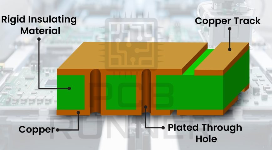
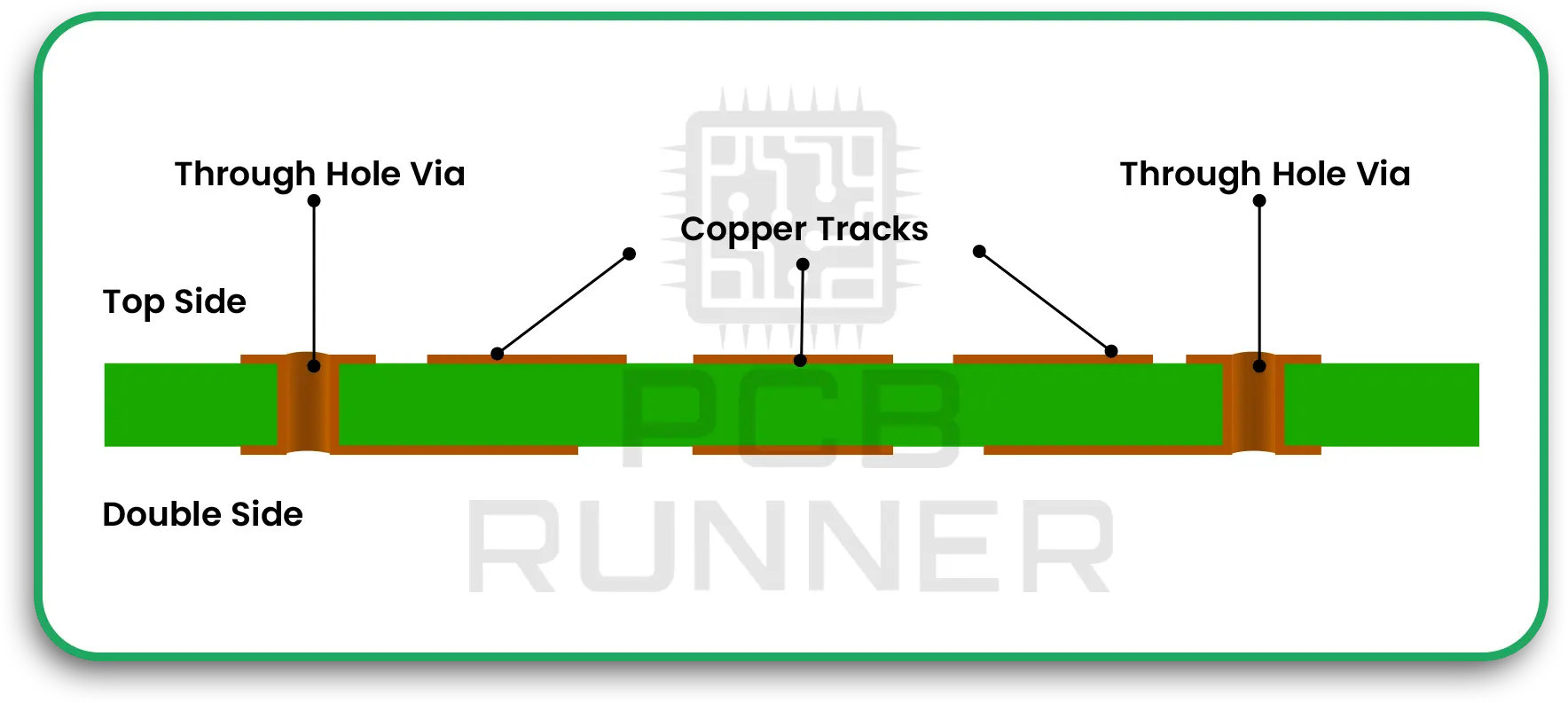
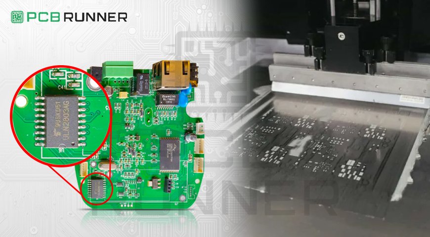
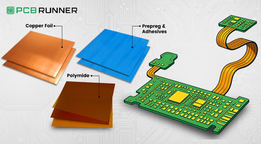
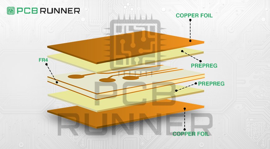
Every call, text, and video stream relies on a telecom pcb. These boards connect and control everything inside your devices, from antennas to processors. As telecom equipment gets more complex, the need for advanced PCB board components and custom PCB with components grows, too.

Today’s telecom PCB assembly isn’t just about putting parts on a board. It’s about building high-speed, high-frequency systems that can handle vast amounts of data. And with 5G rolling out worldwide, the bar is higher than ever.

Why PCBs Matter in Telecom

The Telecom Equipment Market: Growing Fast

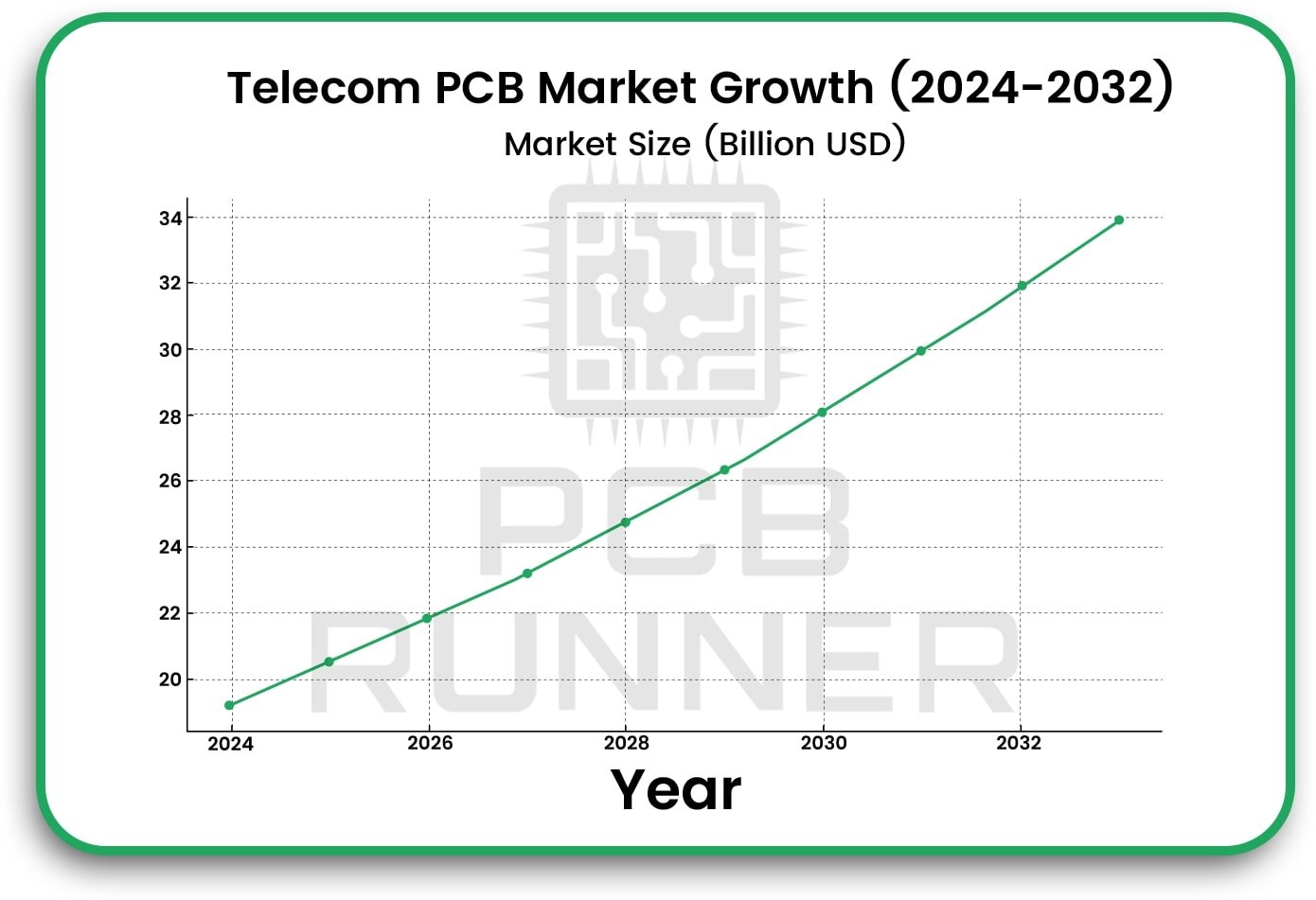
The telecom equipment market is booming. According to recent reports, the telecommunications PCB market is set to grow from about $19.2 billion in 2024 to more than $32 billion by 2033, with a CAGR of 6.5%. That’s a big leap, driven by:

  • The rollout of 5G networks
  • More connected devices (think IoT, smart homes, and cars)
  • The need for faster, more reliable data transfer

But growth brings challenges. Telecom companies need to deliver new products quickly, keep costs down, and make sure every device works perfectly. That’s where PCB manufacturing and supply chain efficiency come in.

The Telecom Equipment Market_ Growing Fast

PCB-Enabled Supply Chain Efficiencies: What Does It Mean?

When we talk about PCB-enabled supply chain efficiencies, we’re talking about every step from design to delivery. It’s about making sure your PCB production uk is fast, flexible, and ready to handle changes, without sacrificing quality.

Here’s how it works:

  • Design for Manufacturability: Start with a PCB layout that’s easy to build and test. Fewer errors mean faster assembly and fewer delays.
  • Local Production: Using PCB production, UK partners can cut shipping times and reduce the risk of global supply chain issues.
  • Smart Sourcing: Work with suppliers who can deliver high-quality PCB component options quickly, even when demand spikes.
  • Integrated Assembly: Choose partners who offer PCB printed circuit board assembly and telecom PCB assembly under one roof. This reduces hand-offs and speeds up delivery.

How PCB Supply Chain Efficiencies Accelerate Telecom Growth

Let’s break it down with real-world benefits:

1. Faster Time to Market

Telecom is a race. If you can launch your product before your competitors, you win more customers. Efficient PCB manufacture and assembly mean you can go from design to finished device in less time. That’s a significant edge in a crowded telecom marketing landscape.

2. Lower Costs

Every delay in the supply chain costs money. By streamlining pcb production uk and using fewer suppliers, you cut costs on shipping, storage, and rework. Plus, with local partners, you avoid the headaches of customs and long-distance logistics.

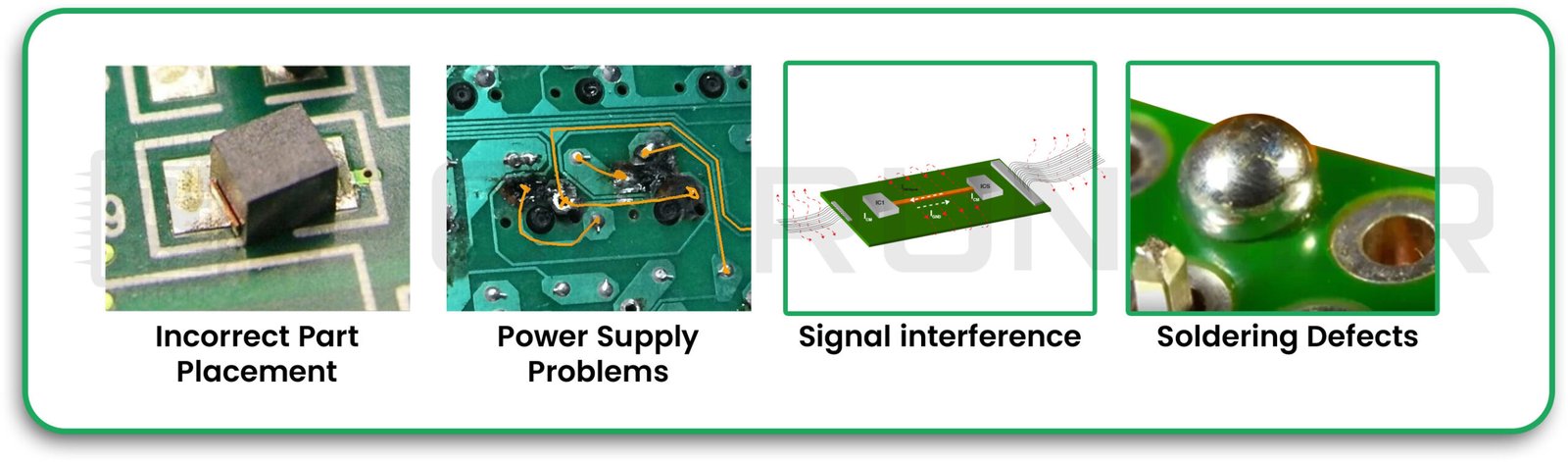
3. Better Quality and Fewer Failures

Mistakes in PCB board components or assembly can lead to device failures, and unhappy customers. Working with experienced telecom PCB assembly teams means fewer errors and more reliable products.

4. Flexibility When You Need It

The telecom equipment market changes fast. Maybe a new standard comes out, or a customer wants a custom PCB with components you haven’t used before. With a smart, flexible supply chain, you can adapt quickly, without missing a beat.

Trends Driving PCB Innovation in Telecom

The printed circuit board industry is not standing still. Here’s what’s shaping the future of telecom pcb:

  • Miniaturization: Devices are getting smaller, but expectations are getting bigger. Advanced PCB component choices and high-density layouts are the new normal1.
  • High-Frequency Materials: 5G and beyond require PCBs that can handle higher speeds and more data4.
  • Green Manufacturing: More companies are looking for eco-friendly pcb manufacture and recyclable materials1.
  • Integrated Solutions: Telecom PCB assembly providers now offer everything from design to final testing, all in one place.

Actionable Tips for Telecom Companies

If you’re in the telecom business, here’s how you can use PCB-enabled supply chain efficiencies to your advantage:

  • Work with local PCB production UK partners to cut lead times and improve communication.
  • Choose assembly partners who specialize in telecom PCB assembly and understand your industry’s unique needs.
  • Invest in design for manufacturability, get your engineers and PCB manufacturing teams talking early.
  • Keep your supply chain flexible by having backup suppliers for key PCB component needs.

Monitor quality at every step, from incoming materials to final PCB printed circuit board assembly.

Final Thoughts

Telecom is all about speed, connection, and reliability. By focusing on PCB-enabled supply chain efficiencies, you can move faster, cut costs, and deliver the high-quality devices your customers expect. Whether you’re launching the next big thing in 5G or just looking to improve your current products, the right approach to PCB manufacture and assembly will help you stay ahead in the telecom equipment market.

Keep your supply chain smart, flexible, and focused on quality, and watch your business grow.

FAQs: Telecom PCBs and Supply Chain Efficiencies

1. Why is PCB manufacturing so important for telecom?
PCBs are the foundation of every telecom device. Fast, reliable manufacture means quicker launches and better products.
2. How does PCB production UK help with supply chain issues?
Local production cuts shipping times, avoids customs delays, and makes it easier to solve problems quickly.
3. What makes telecom PCB assembly different from other industries?
Telecom PCBs need to handle high speeds, lots of data, and demanding reliability standards. Assembly partners must have experience with these demands.
4. What are the key PCB board components in telecom devices?
Common components include processors, memory chips, power management ICs, and high-frequency connectors.
5. How can I make my supply chain more flexible?
Work with multiple suppliers, keep extra stock of critical PCB component parts and choose partners who can handle changes fast.
6. What’s the benefit of a custom pcb with components for telecom?
Custom PCBs allow you to design exactly what you need, improving device performance and reducing size.
7. How does supply chain efficiency impact telecom marketing?
Faster launches and better products help you stand out in the telecom marketing world, winning more customers.
8. What’s the outlook for the telecom equipment market?
With 5G, IoT, and smart devices growing fast, the telecom equipment market is set for strong growth in the next decade.

Double-Sided PCBs

How Double-Sided PCBs Improve Performance & Reduce Size

Have you ever wondered how modern electronics keep getting smaller and more powerful at the same time? Are you building a compact device and worried about fitting all your parts onto one board? Or maybe you’re trying to boost performance without increasing the size. If so, you’re not alone. These are common concerns when working with circuit boards, and double-sided PCBs might be just what you need.

What Is a Double-Sided PCB?

A double-sided PCB is a printed circuit board with copper layers on both the top and bottom. This means you can place components on both sides. That gives you more space and more options when designing your circuit. Unlike a single-sided board, which only has copper on one side, a double-sided PCB lets you connect parts in a more compact and flexible way.

Double sided board

Why Should You Use a Double-Sided PCB Board?

If you’re designing something like a smart device or sensor that needs to be small but fast, a double-sided PCB board can help. Here’s why many people choose them:

  • You get more space for parts: You can place parts on both sides instead of just one.
  • Your circuits work better: Signals can travel shorter paths, which helps improve speed and reliability.
  • They cost less than multilayer boards: You get better performance without paying as much as you would for more complex boards.

Real Benefits of Double-Sided PCB Assembly

Double-sided PCB (Printed Circuit Board) assembly is an essential technique in modern electronics. It involves placing electronic components on both the top and bottom sides of the board. This approach offers several practical benefits that make it a popular choice for many applications. Let’s break down why double-sided PCB assembly is so useful:

1. Better Performance

One of the biggest advantages is better performance. When signals don’t have to travel as far across the board, resistance is lower, and the speed of signal transmission increases. This means that your device can operate more efficiently and respond faster. For example, in devices like smartphones or gaming consoles, quick data transfer is crucial, and double-sided PCBs help achieve that.

2. Smaller Designs

Another major benefit is the ability to create smaller designs. By utilising both sides of the PCB, you can fit more components into a limited space. This is particularly valuable for compact gadgets like smartwatches, fitness trackers, or advanced medical devices, where saving space without sacrificing performance is essential. As technology becomes more compact, double-sided PCB assembly allows engineers to meet these size constraints effectively.

3. Even Heat Spread

In addition to size and performance, double-sided PCBs also offer improved heat management. Since components are distributed on both sides, heat can spread out more evenly, preventing hotspots and reducing the risk of overheating. This balanced heat dissipation ensures that the board stays reliable over time, even in demanding applications like industrial machinery or high-performance computing devices.

4. Flexible Layouts

Moreover, double-sided PCB assembly provides greater flexibility when designing circuit layouts. The extra surface area on both sides gives engineers more options for routing power and signal paths. This means that complex circuits can be designed with fewer compromises, allowing for more efficient and organised component placement. As a result, products can be developed with enhanced functionality while maintaining a sleek, compact form factor.

Where Are Double-Sided PCBs Used?

Double-sided PCBs show up in a lot of products. Here are some common examples:

  • Phones and tablets: To keep them slim while still packing power.
  • Cars: For control panels, cameras, and safety systems.
  • Factories: Machines use these boards in their control units.
  • Medical gear: For small tools that track or check health.

Why Choosing the Right PCB Manufacturer Matters

When you’re ready to build a double-sided board, working with the right team is key. Not all PCB manufacturers are the same. A skilled PCB manufacturer can help you avoid problems and build a board that really works.

Here’s what to look for:

  • Experience with double-sided PCB assembly
  • Ability to meet deadlines
  • Support with custom printed circuit board designs
  • Good materials and quality checks

You want someone who listens to your needs and delivers solid work.

When You Need a Custom Printed Circuit Board

No two projects are exactly alike. That’s why going custom can be a big help. A custom printed circuit board fits your exact needs, from the shape of the board to the thickness of the copper.

Custom boards let you:

  • Pick your own layout and shape
  • Decide how much power to handle
  • Choose special materials for heat or strength

This kind of flexibility means your design can be faster, smaller, and tougher.

Start With a Double-Sided PCB Board Prototype

Before you make 1,000 boards, it’s smart to test one. That’s what a double-sided PCB board prototype is for. A prototype lets you see how the board fits, works, and holds up in real use.

Fast prototyping helps you catch mistakes early. Good pcb manufacturers can get you a working sample fast, so you stay on schedule.

Why PCB Manufacturers Should Offer Fast Prototyping

Time is important. Delays cost money. That’s why it’s helpful to work with a team that offers fast PCB prototyping. Speed helps you:

  • Test ideas quickly
  • Fix problems early
  • Launch your product faster

Some of the best pcb manufacturers offer 24–72 hour turnaround times on prototypes. That gives you more time to focus on the rest of your project.

Comparing Double-Sided to Other PCB Types

Feature Single-Sided PCB Double-Sided PCB Multilayer PCB
Component Mounting One side only Both sides Multiple inner layers
Cost Low Medium High
Complexity Supported Low Medium High
Space Efficiency Low High Very High
Used In Simple gadgets Phones, tools Servers, routers

As you can see, double-sided boards are the perfect middle ground. They offer more power than basic boards but don’t cost as much as multilayer ones.

What Is Double-Sided PCB Jump Scoring?

Sometimes, a large double-sided PCB needs to be broken into smaller parts. That’s where PCB jump scoring helps. It’s a method where grooves are made on both sides of the board so you can snap parts apart cleanly.

Jump scoring is useful if:

  • You’re making panels of small boards
  • You need easy break-off sections

Ask your PCB assembler if they offer this service, especially for high-volume jobs.

Choosing a PCB Assembler for Your Project

Once your design is ready, a pcb assembler takes the parts and puts them on your board. You want someone with experience in double sided PCB assembly.

Look for:

  • Good reviews and past work
  • Fast service times
  • Support with testing

A reliable assembler means fewer headaches and better boards.

Final Thoughts

Double-sided PCBs offer a smart way to make your devices smaller and more powerful. They’re great for phones, tools, cars, and more. You get better signal flow, smaller size, and improved heat control.

To get started, work with experienced printed circuit board manufacturers. Whether you need a custom printed circuit board, a fast double sided PCB board prototype, or jump scoring, the right partner will guide you every step of the way.

If you’re ready to upgrade your design, reach out to a trusted pcb manufacturer or pcb assembler today like PCB Runner. Your next smart device might just start with a smarter board.

Prototyping for New Hardware

A Practical Guide to Prototyping for New Hardware Ventures

If you’re building a new piece of hardware, you can’t skip the prototyping stage. A prototype helps you test your idea and see if it works in the real world. It’s a small, working version of your product. For electronics, this means using a PCB board prototype. Prototyping helps you find problems early, save money, and build confidence in your design before full production.

This blog will serve as a guide for new hardware ventures prototyping.

What is a PCB Prototype?

A PCB board prototype is a sample of a printed circuit board (PCB) created to test your circuit design. You use it to check if your idea works before making large quantities. It’s like baking a small batch of cookies to see if the recipe is good. A PCB prototype board helps you avoid costly mistakes. It shows you what needs fixing before your idea hits the market.

Step 1: Choosing the Right PCB Manufacturer

Before making a prototype, you need a PCB manufacturer who can work with you on small, quick batches. Not all PCB circuit board manufacturers are the same. Look for one like PCB Runner, which offers fast turnaround and supports both prototypes and large-scale production. PCB Runner has been serving the UK and European industries for over a decade, handling critical electronics for sectors like aerospace and medical.

What to Look For:

  • Ability to handle fast PCB prototyping
  • Experience with prototype PCB assembly
  • Quality certifications like ISO9001
  • Support for design file checks and one-on-one customer service

Step 2: Designing Your Prototype

Designing your prototype means creating a layout for your circuit. You’ll use special software for this. Most hobbyists and engineers use tools like Kicad, Eagle, or Altium.

Tips for Good Design:

  • Keep your layout simple for the first version
  • Use components that are easy to find and solder
  • Label all your parts clearly on the board

Your goal here isn’t perfection. It’s to get a working version that shows your idea in action.

Step 3: Submitting Your Files

Once your design is ready, send your Gerber files to your chosen PCB manufacturer. Gerber files are like blueprints for your board. They tell the manufacturer where to place copper, holes, and other layers.

What You Should Send:

  • Gerber files
  • Bill of Materials (BOM)
  • Pick and place file for prototype PCB assembly

Good manufacturers like PCB Runner offer engineering review for free. They’ll check your files to make sure everything is correct before starting production.

Step 4: Fast PCB Prototyping

Time matters in hardware. If your project has a deadline or you’re trying to beat competitors to market, you need fast PCB prototyping. PCB Runner offers quick-turn manufacturing, meaning your boards are ready in just a few days.

Benefits of Fast Prototyping:

  • Quick testing and feedback
  • Faster updates to the next version
  • Less time wasted waiting on parts

Step 5: Assembly and Testing

After your boards are fabricated, the next step is prototype PCB assembly. This means placing the electronic components on the board. You can do this yourself or have your manufacturer assemble it for you.

Choose Professional Assembly If:

  • Your board has small or complex components
  • You want to save time
  • You need multiple units tested

Once assembled, test your board thoroughly. Check every function and log any issues.

Common Issues During Prototyping

Even if you follow all the steps, you might run into problems. That’s okay. It’s part of the process.

Issues You Might See:

  • Incorrect part placement
  • Power supply problems
  • Signal interference
  • Soldering defects

Take notes and update your design before ordering your next version. PCB Runner helps here too, offering support from real people with experience.

Common issues During Prototype

Iteration: Making Your Next Version

The prototype is rarely the final version. You’ll likely need two or three rounds of prototyping. This helps improve performance, reduce size, or cut costs. With each version, your design gets stronger and more ready for the market.

How to Speed Up Iteration:
  • Keep a checklist of problems
  • Use only what you need on the board
  • Partner with reliable PCB circuit board manufacturers like PCB Runner

Real-World Example

Let’s say you’re building a smart temperature sensor. Your prototype might be large and use basic parts. After testing, you find that the sensor is slow to respond. In the next version, you choose a better chip and shorten the signal path. Now it works faster and uses less power. That’s the power of prototyping.

Why Choose PCB Runner for Prototypes?

PCB Runner is trusted by startups, hobbyists, and engineers across the UK and Europe. They specialise in both PCB board prototype and full production.

What They Offer:

  • Quick-turn prototyping
  • Support for fast PCB prototyping
  • One-stop service from fabrication to assembly
  • Free file review before production
  • Reliable customer support, 24/7

With their in-house manufacturing and ISO certification, you know your boards are made to high standards.

Final Tips Before You Start

  1. Don’t overthink your first version: Start simple and focus on making it work. Your first version doesn’t need to be perfect. The goal is to have a working prototype that you can improve later. Keep it basic and functional.
  2. Test your board in real conditions: Make sure to test your PCB in the actual environment where it will be used. This helps you identify any issues related to temperature, humidity, or electrical interference early on. Real-world testing can save you from unexpected problems after production.
  3. Work with a full-service provider: Save time and hassle by partnering with a reliable provider like PCB Runner. They can handle everything from design to manufacturing, helping you avoid common pitfalls and ensuring a smoother process.
  4. Don’t hesitate to ask for help: If you’re unsure about something, reach out for assistance. A reputable PCB manufacturer will offer guidance and support throughout the process, whether it’s about design specifications, material choices, or quality testing.

Conclusion

Prototyping is a must for anyone working on new electronics. It helps you test your idea, fix problems, and get to market faster. Whether you’re a beginner or an experienced builder, starting with a solid PCB board prototype is key. With expert help from PCB circuit board manufacturers like PCB Runner, you can go from idea to product with confidence. From PCB prototype board to prototype PCB assembly, they’ll help you every step of the way. Don’t wait, start your hardware journey today.

Need a fast quote or want to upload your files? PCB Runner is ready to help 24/7.

Solder Paste Masks

How Solder Paste Masks Improve PCB Reliability and Performance

When working with any printed circuit board (PCB), one important detail you should never overlook is the solder paste mask. While it may seem like a thin layer of colour on the board, the paste mask plays a key role in how well your board works. It impacts everything from the board’s strength to how it performs under stress.

In this blog, you will learn how solder paste masks work, what materials are used, and why they matter so much. You will also see how these masks support high-density interconnect designs and improve your PCB board assembly process.

What Is a Solder Paste Mask?

A solder paste mask, often simply called a solder mask, is a protective layer placed on a PCB. This layer covers the areas where you do not want the solder to stick. It also leaves openings where you want the solder to go during the assembly process.

The most common type of solder mask is made using epoxy or liquid photoimageable (LPI) solder mask material. These materials are chosen for their ability to stick well to the board and for how well they resist heat and moisture.

Solder Paste Mask

Why Use a Solder Paste Mask?

You might wonder why you even need this layer. Here are a few reasons:

  • Prevents solder bridging: It keeps solder from connecting parts that should not be connected.

Solder Bridge

  • Improves board durability: It protects the board from moisture, dust, and other damage.

Improves board durability

  • Helps with PCB solder mask alignment: It ensures solder goes only where it should during reflow.

smd & nsmd pad

Without a solder mask, your PCB can short out more easily or wear down faster. So, even though it is a small part of the board, it has a significant impact.

Types of Solder Mask Materials

There are different types of solder mask materials, and the right one depends on how your board will be used:

  1. Epoxy liquid: This is a lower-cost option. It is applied with a screen printing method. It works well for simple PCBs.
  2. LPI (Liquid Photoimageable): This is the most common option for modern circuit boards. It gives better accuracy, especially for high-density interconnect boards.
  3. Dry film: This is used when the board design needs very tight spacing and high resolution.

When you choose the best solder mask material for your project, you help improve the life and performance of your circuit board.

Paste Mask in PCB: What Does It Do?

The paste mask is closely related to the solder mask, but they are not the same thing. The paste mask defines where solder paste should be applied. This happens before the board is placed in a reflow oven.

The paste mask ensures that paste is applied only to pad areas, not on traces or open board space. This step is crucial when your design includes a high number of small parts, like in a high-density interconnect board.

How the Solder Mask Helps in PCB Board Assembly

During PCB board assembly, accurate paste placement is critical. The solder mask keeps paste from flowing into unwanted areas. This protects nearby parts from getting too much heat or unwanted solder during reflow.

In boards with small components or tight spacing, like those made by advanced pcb circuit board manufacturers, this becomes even more important. Paste mask and solder mask work together to make sure assembly is smooth and your board ends up strong.

Board Paste Flow and Control

One key benefit of having a good solder paste mask setup is better control of paste flow. When the paste goes only where it should, you get stronger joints, fewer solder balls, and less chance of failure.

For example, on a high-density interconnect board, solder mask openings must be exact. Even small mistakes in the opening size or placement can lead to solder bridges or weak connections. Using the right paste mask in PCB design keeps those problems from happening.

PCB Solder Mask Colors and What They Mean

While green is the most common colour, solder masks also come in red, blue, white, black, and other shades. These colours are mostly for looks or specific lighting requirements during testing and inspection.

However, you should know that some colours make visual inspection easier. For example, green shows contrast better for human eyes, which can be helpful during manual checking.

Some PCB manufacturers offer custom solder mask colours to fit brand or functional needs.

Solder Mask Design Tips

Here are a few helpful tips when working on your board’s solder mask:

  • Match it with pad sizes: Keep the mask opening slightly larger than the pad to allow for placement tolerance.
  • Use solder mask relief: This keeps the mask from peeling or lifting over time.
  • Review high-density zones carefully: Pay close attention to BGA and fine-pitch parts.

Making the right design choices for solder masks saves you from costly fixes later in the process.

What Happens If You Skip the Solder Mask?

You might think of skipping the solder mask if your board has very few parts. But doing so can lead to:

  • Short circuits
  • Moisture damage
  • Poor solder quality
  • Decreased product lifespan

Even simple boards benefit from this extra protection. Most pc board manufacturers will include it as part of standard PCB fabrication.

Role in High-Density Interconnect Boards

When it comes to high-density interconnect PCBs, solder mask design becomes critical. These boards pack more connections in less space. That means paste and solder have very little room for error.

The solder mask helps guide the paste to the correct locations. This prevents bridging or weak joints, even when using microvias and tiny SMD parts.

So, if you are working with a high-density interconnect board, pay close attention to your solder mask layer. It could make or break your board’s reliability.

Trust PCB Runner for Quality PCB Board Assembly

If you want a PCB that works the first time and lasts long, do not ignore your solder paste mask. It protects your board, controls solder flow, and ensures clean assembly.

Whether you need simple boards or complex high-density interconnect solutions, getting the solder mask right is key.

At PCB Runner, we focus on quality from start to finish. Our team pays close attention to every detail, including solder mask material, board paste control, and paste mask alignment. As experienced PCB circuit board manufacturers, we ensure your PCB board assembly meets the highest standards.

Contact PCB Runner today to learn how we can help with your next project. Your board’s performance starts with smart choices in every layer.

SMT Efficiency with Premium Laser Cut Stencils

Improve SMT Efficiency with Premium Laser Cut Stencils

If you want clean solder joints and fewer errors in your circuit board assembly process, you need to pay attention to your stencils. Laser-cut stencils can make a big difference when it comes to surface mount technology (SMT) work. Whether you’re a PCB assembler or running a full-service PCB fabrication shop, the stencil you use matters more than you might think.

This blog will discuss how premium laser-cut stencils help boost SMT efficiency, reduce waste, and improve the final quality of your assemblies. We’ll also explain how they work, why thickness matters, and how they affect surface mount device soldering.

What Is a Laser Cut Stencil?

A laser-cut stencil is a thin sheet of metal, usually stainless steel, with openings that match your printed circuit board’s solder pad layout. It’s used during the SMT process to apply solder paste accurately onto the pads. Once the solder paste is applied through the stencil, your surface mount components are placed on top before the board goes through the reflow oven.

Laser cut stencils are created using precise lasers that ensure every opening is sharp and clean. Unlike older stencils made using chemical etching, laser-cut stencils give you better control over the paste volume and alignment. This makes them the first choice for most modern PCB assemblers.

Laser Cut Stencil

Why Are Laser Cut Stencils Better?

If you’re wondering why these stencils are considered premium, here’s why:

  • Better Accuracy: Laser machines cut immaculate edges, which means your paste is applied precisely where it’s needed.
  • Consistent Paste Volume: Uniform openings ensure the same amount of solder paste is applied to every pad.
  • Fewer Bridges and Voids: Better paste control reduces soldering issues like bridging and voids.
  • Repeatability: You get the same great results every time, which helps reduce errors in mass production.

All these benefits lead to fewer touch-ups and rework later on.

PCB Stencil Thickness: Why It Matters

The thickness of your stencil has a significant impact on how well the solder paste is deposited. Too thick, and you might end up with too much paste, causing short circuits or bridging. Too thin, and you may not get enough solder paste, leading to weak joints or poor connections.

Most standard SMT stencils are around 0.1 mm to 0.15 mm thick. The proper thickness depends on the size and type of surface mount devices you’re using. For fine-pitch components or small pads, a thinner stencil is often the better choice.

Talk to your PCB assembler or circuit board assembly team about what stencil thickness works best for your project. Picking the proper thickness will reduce paste-related issues and improve yield.

pcb stancil thickness

Laser Cut Stencils and Surface Mount Device Soldering

Soldering small components like resistors, capacitors, and ICs is all about precision. Surface mount device soldering needs just the right amount of paste in the right place. Laser cut stencils help make this possible by giving you tighter control over paste placement.

When your paste is applied cleanly, components stay in place better during reflow. It also ensures strong joints once the solder melts and hardens. That’s how you get reliable connections that stand up to heat, vibration, and other stresses.

laser cut stancil Surface Mount soldering

Why PCB Assemblers Rely on Premium Stencils

If you’re working with a professional PCB assembler, you’ll likely hear them mention the importance of a good stencil. That’s because:

  • Stencils save time on manual paste application
  • They cut down on waste and scrap boards
  • They support consistent results across production runs

For high-mix, low-volume jobs or full-scale production, investing in a quality stencil just makes sense. You spend less time fixing problems and more time shipping working boards.

Key Tips for Choosing the Right Stencil

Selecting the correct stencil for your surface mount technology (SMT) process is crucial for consistent solder paste deposition and overall PCB assembly quality. A poorly chosen or maintained stencil can result in misalignment, insufficient or excessive solder, and costly rework. Below are the key tips to help you make the best stencil choice for your production needs.

1. Match the Stencil Thickness to Your Component Sizes

Stencil thickness directly affects the amount of solder paste deposited during the printing process. Thicker stencils (e.g., 0.15–0.20 mm) are suitable for larger components like connectors or power devices, while thinner stencils (e.g., 0.10–0.12 mm) are ideal for fine-pitch components such as QFNs or micro BGAs. If the thickness is not matched correctly, it can lead to solder bridging or insufficient solder joints. Always consider the smallest aperture and component pitch when determining the appropriate thickness.

2. Use Laser-Cut Stencils for Finer Accuracy

Laser-cut stainless steel stencils offer the highest precision and consistency, especially for complex and high-density SMT boards. They produce cleaner aperture walls, which helps in achieving uniform paste release. For critical applications with 0.5 mm or smaller pitch components, laser cutting is the preferred method. Electro-polished laser-cut stencils can further enhance paste transfer efficiency and reduce defects like solder beading or bridging.

3. Avoid Worn or Dirty Stencils to Prevent Smearing or Clogging

Stencil wear over time can lead to distorted apertures, clogged openings, or uneven paste application. Dirt, dried paste, or even moisture can also cause smearing, resulting in shorts and open circuits on the board. Regular inspection and cleaning of stencils are essential to maintain print quality. Automated stencil cleaners or manual cleaning with appropriate solvents can extend stencil life and ensure consistent results.

4. Store Stencils Flat and Clean to Maintain Shape

Improper stencil storage , such as bending, stacking, or exposure to dust , can warp the metal, damage apertures, or cause misalignment during printing. Stencils should always be stored flat in protective sleeves or frames in a clean, climate-controlled environment. Following proper handling and storage protocols helps maintain stencil integrity and prolongs its usability over multiple production cycles.

Work with a Trusted PCB Fabrication Partner Who Understands SMT Needs

Your stencil quality is only as good as the partner you work with. Collaborating with an experienced PCB fabrication and assembly provider ensures that your stencils are manufactured to exact specifications. A reliable partner will help you choose the right aperture design, thickness, and finish based on your specific component layout and soldering process. They can also advise on stencil design modifications, such as step-down regions or nano-coatings, for challenging applications.

From PCB Fabrication to Assembly: How Stencils Fit In

Your PCB fabrication process lays the groundwork. Once you get your board made, the next step is assembly. That’s where stencils come in. Whether you’re working with rigid, flex, or hybrid boards, having a proper stencil helps your assembly run smoother.

Some pc board manufacturers also offer stencil services alongside fabrication. If you’re placing an order with a PCB circuit board manufacturer, ask if they can supply a matching laser-cut stencil. That way, you can avoid delays and get a stencil that perfectly fits your layout.

Final Thoughts: Why It’s Worth It

Good stencils are not just extra tools. They are a must-have for efficient, accurate SMT. Using premium laser cut stencils helps you:

  • Reduce soldering errors
  • Improve product quality
  • Lower assembly costs

If you want to get the most out of your circuit board assembly process, it’s worth choosing the right tools from the start. Laser cut stencils are one of those tools that give you better results without extra effort.

Talk to your PCB assembler or supplier about including laser stencils in your next order. A small step like this can go a long way in boosting your productivity.

V-Scoring in PCB Manufacturing

Why V-Scoring Is Essential in PCB Manufacturing?

Printed circuit boards (PCBs) are at the heart of almost every electronic device. But what happens before they get to your hands? A lot of planning, cutting, and assembling takes place. A critical part of the manufacturing process is something called V-scoring. If you’re building your electronics or just curious about how things work, this blog will help you understand why V-scoring is so vital in PCB manufacturing.

What Is V-Scoring in PCB Manufacturing?

V-scoring is a method used by PCB manufacturers to help separate individual circuit boards from a larger panel. Imagine baking a batch of cookies and then cutting them into pieces before serving. That’s pretty much what V-scoring does only with circuit boards.

It involves making V-shaped grooves on both sides of the board. These grooves are not deep enough to cut all the way through. Instead, they make it easier to snap the boards apart cleanly after assembly.

V-Scoring

Why Use Panels Instead of Single Boards?

When PCB assemblers make multiple boards at once, they put them all in one large panel. This helps with quicker assembly and better handling. Handling single boards one at a time would be slow and costly. That’s why PCB board manufacturers often design multiple boards on a single panel.

Once everything is soldered and tested, the boards are separated. That’s where V-scoring or other methods like routing come in. But V-scoring is often faster and cheaper.

Benefits of V-Scoring for PCB Assemblers

1. Faster Assembly

It’s easier to work on a panel with several boards than on single pieces. Pick-and-place machines can handle them more quickly.

2. Easy Separation

After assembly, the boards can be snapped apart easily without special tools.

3. Cost-Effective

It uses less space and fewer tools, which means lower costs.

4. Less Waste

V-scoring makes better use of board material. Less waste is always a good thing!

How Does V-Scoring Work?

V-scoring works by cutting shallow V-shaped grooves into both the top and bottom of the board. These grooves weaken the board just enough to let it snap apart when needed. But they still leave the panel strong enough to handle during assembly.

V-Scoring vs. PCB Jump Scoring

You might also hear about something called PCB jump scoring. This is a special kind of V-scoring where the groove doesn’t run all the way across the board. Instead, it “jumps” over sensitive areas. This helps protect certain parts while still allowing for separation.

Both V-scoring and jump scoring are used by professional PCB assemblers, depending on the design and purpose of the board.

V-Scoring vs. PCB Jump Scoring

When Should You Use V-Scoring?

V-scoring works best when your boards:

  • Are rectangular
  • Need to be mass-produced.
  • Don’t have sensitive components near the edges.

If your design is round or has curves, other options like routing might be better.

What Should You Know Before Using V-Scoring?

If you’re working with a PCB board manufacturer, here are a few things to keep in mind:

  1. Spacing: Keep components away from the edge of the board. That way, they don’t get damaged when the board is snapped apart.
  2. Panel Thickness: V-scoring works best on panels that are not too thick. Most manufacturers will let you know what thickness is best.
  3. V-Score Angle and Depth: These are usually 30 to 45 degrees and should go about one-third into the board from each side. Ask your manufacturer for their specific limits.
  4. PCB Design Files: Make sure your files clearly show where you want the V-scores. Most PCB manufacturers have design rules for this.

Real-Life Uses of V-Scoring

  • Consumer Electronics: Phones, tablets, and laptops often use panels with V-scored boards to speed up production.
  • Industrial Machines: Panels make it easier to handle boards during rougher assembly conditions.
  • LED Lighting: LED strips and panels often use V-scoring for quick snapping into smaller units.

Common Mistakes to Avoid

  1. Placing Parts Too Close to the Edge: These parts might break during snapping.
  2. Not Using the Right Thickness: Boards that are too thick might not snap cleanly.
  3. Not Testing the Separation Method: Always test one panel before full production.

How PCB Runner Handles V-Scoring

Top UK PCB Manufacturer: PCB Runner

PCB Runner has been a trusted PCB manufacturer and PCB assembler in the UK and Europe for over 10 years. Whether you’re working on a custom PCB or a whole circuit board assembly, we handle everything under one roof.

With PCB Runner, you don’t need to worry about your V-scoring requirements. Our team checks your files and helps you decide the best method for board separation. We don’t just manufacture; we also support your design process. We even offer 24-hour tech support so that you can get help anytime.

Our facility is certified with ISO9001 and qualified for IPC Class 2, 3, and 3A. We serve industries like aerospace, defence, medical, and more. Whether your boards are for hobby projects or critical systems, PCB Runner delivers quality.

We also support advanced features like PCB jump scoring when your design needs special care. If your design includes delicate components near the edge, we can work with you to avoid damage during board separation.

Conclusion: V-Scoring Makes a Big Difference

V-scoring may seem like a small part of the PCB manufacturing process, but it plays a massive role in making things faster, cheaper, and more reliable. If you’re planning to get boards made, ask your PCB board manufacturer about V-scoring. It might be just the feature you need.

Working with an experienced partner like PCB Runner makes everything easier. We understand every detail, from circuit board assembly to advanced scoring techniques. Whether you’re a beginner or a pro, our team is here to help you every step of the way.

So next time you order PCBs, don’t forget to ask about V-scoring. It could save you time, money, and stress.

Need help with V-scoring or anything else PCB-related? Get in touch with PCB Runner today for expert advice and a free quote. Upload your Gerber files and see how easy and efficient PCB manufacturing can be!

Electronic Board Manufacturer

Leading Electronic Board Manufacturer in the UK – PCB Runner

Welcome to PCB Runner, your trusted partner for all things related to electronic board manufacturing in the UK. If you are looking for a reliable PCB manufacturer that delivers high-quality multilayer printed circuit boards, you are in the right place. In this blog, we will explore what makes PCB Runner a leader among printed circuit board manufacturers in the UK, what services we offer, and why choosing the right electronic PCB board manufacturer matters for your business.

What is a Printed Circuit Board (PCB)?

A printed circuit board (PCB) is the backbone of almost every electronic device. It connects and supports electronic components using conductive tracks, pads, and other features etched from copper sheets laminated onto a non-conductive substrate. Whether you are using a smartphone, a computer, or a medical device, PCB board electronics are at the heart of its operation.

Why PCB Runner is the Leading PCB Manufacturer in the UK

Experience and Expertise

PCB Runner has been a top electronic board manufacturing company for over 10 years. We serve a wide range of industries, including military, aerospace, defence, medical, and more. Our team understands the importance of delivering reliable and high-quality electronic PCB boards on time.

Certified Quality

We are an ISO9001 certified PCB manufacturer, and our boards meet IPC Class 2, 3, and 3A standards. This means you get consistent quality with every order. Our certifications show our commitment to quality and reliability, which is why many customers trust us for their critical applications.

One-Stop Solution

PCB Runner offers all services under one roof. From design to multilayer printed circuit board manufacturing and assembly, you get everything you need in one place. This single-window service saves you time and ensures smooth project management.

Our Electronic Board Manufacturing Services

Multilayer Printed Circuit Board Manufacturing

Multilayer PCBs have more than two layers of conductive material. These boards are perfect for complex circuits that need to fit in small spaces. They are stronger, more durable, and allow for higher speed and capacity. At PCB Runner, we specialize in multilayer printed circuit board manufacturing for demanding applications.

Benefits of Multilayer PCBs:

  • Compact size for complex designs
  • Improved durability and reliability
  • Better performance for high-speed circuits
  • Space-saving for modern electronics

PCB Assembly Services

We do not just manufacture PCBs; we also offer professional assembly services. Our team assembles components onto your boards with precision, ensuring your electronic PCB board works perfectly from the start.

Quick Turnaround

Need your boards fast? PCB Runner specializes in quick-turn manufacturing for both small and large quantities. We understand that time is critical, so we deliver your PCB board electronics quickly without compromising on quality.

24-Hour Tech Support

Whenever you need help, our 24-hour tech support is just a call away. You will always speak to a real person who can answer your questions and solve any issues you might have.

Instant Quotes and Easy Ordering

Getting a quote is easy and instant. You can order, reorder, upload your files, and get status updates online at any time. This makes the process smooth and hassle-free for all our customers.

Why Choose PCB Runner Over Other Printed Circuit Board Manufacturers UK?

  • Reliability: We do what we promise. Our customers trust us because we deliver on time and meet their needs every time.
  • Quality Assurance: We review all engineering files before starting production to ensure you get exactly what you expect. There are no extra charges for this review.
  • Customer Service: Our team is always ready to help, whether you need technical advice or support after your order.
  • Trusted by Many: Many of our new customers come through referrals from satisfied clients. We have earned the trust of several OEMs who depend on us for their electronic board manufacturing needs.

How PCB Runner Supports Different Industries

PCB Runner serves a wide range of industries that require high-quality multilayer printed circuit boards and electronic PCB board solutions. Here are some of the industries we support:

Our experience with critical and demanding applications makes us a preferred electronic PCB board manufacturer for businesses that cannot afford to compromise on quality.

The PCB Manufacturing Process: Simple Steps

Here’s a quick look at how we make your PCB board electronics:

  1. Design Review: We check your engineering files for accuracy and manufacturability.
  2. Material Selection: We use high-quality materials for all boards, including exotic options for special needs.
  3. Layer Construction: For multilayer printed circuit boards, we stack and bond several layers together for strength and performance.
  4. Drilling and Plating: We drill holes and plate them to connect different layers.
  5. Etching and Solder Mask: We etch the copper to create circuits and add a solder mask for protection.
  6. Assembly: Components are placed and soldered onto your board.
  7. Testing: Each board is tested for quality and performance before shipping.

What Makes Multilayer Printed Circuit Boards Special?

Multilayer printed circuit boards are essential for modern electronics. They allow for more complex circuits in smaller spaces. Here’s why they are often chosen over single or double-sided boards:

  • Space Efficiency: Multiple layers mean more circuits in less space.
  • Improved Performance: Better for high-speed and high-capacity devices.
  • Durability: More layers add strength and reliability.
  • Single Power Input: Unlike using several single-layer boards, a multilayer board usually needs just one power connection.


Single-Sided vs. Double-Sided vs. Multilayer PCBs

Feature Single-Sided PCB Double-Sided PCB Multilayer PCB
Number of Layers 1 2 3 or more
Complexity Low Medium High
Size Larger Medium Smallest
Cost Lowest Moderate Higher
Application Simple devices Moderate devices Advanced electronics
Durability Basic Good Best

Conclusion

PCB Runner stands out as a leading printed circuit board manufacturer in the UK because of our commitment to quality, reliability, and customer service. Whether you need a simple electronic PCB board or a complex multilayer printed circuit board, we have the skills and experience to deliver what you need on time and at the right price.

If you are looking for a trustworthy electronic PCB board manufacturer for your next project, contact PCB Runner today for a free quote. Let us help you bring your ideas to life with the best in electronic board manufacturing.

Ready to get started?

Contact PCB Runner now for your instant quote and experience the difference of working with a true leader in the UK PCB industry.

Frequently Asked Questions (FAQs)

nt quote and experience the difference of working with a true leader in the UK PCB industry.

Q1: What is a multilayer printed circuit board?
A multilayer printed circuit board has three or more layers of conductive material. These layers are stacked and bonded together, allowing for complex and compact electronic designs.

Q2: Why should I choose a UK-based PCB manufacturer?
Choosing a UK-based PCB manufacturer like PCB Runner ensures faster communication, quicker delivery, and better support. You also get the advantage of strict quality standards.

Q3: Can I get both PCB manufacturing and assembly services at PCB Runner?
Yes, PCB Runner offers both manufacturing and assembly under one roof. This makes your project easier to manage and ensures better quality control.

Q4: How fast can I get my PCBs delivered?
We specialize in quick-turn services and can deliver both small and large quantities quickly, depending on your needs.

Q5: What industries do you serve?
We serve a wide range of industries, including military, aerospace, medical, industrial, and consumer electronics. Our expertise covers both simple and complex electronic board manufacturing needs.

Rigid-Flex PCB

Rigid-Flex PCBs: Best Materials and Manufacturing Methods

Rigid-flex PCBs are changing how we design electronic devices. By combining flexible and rigid sections, they allow for compact, durable, and reliable products. If you’re working on a project that requires space-saving and robust circuit boards, understanding the materials and manufacturing processes is crucial.

Understanding Rigid-Flex PCBs

A rigid-flex PCB integrates both rigid and flexible substrates into a single board. The rigid parts provide structural support and house components, while the flexible sections connect different rigid parts, allowing the board to bend and fit into tight spaces. This design reduces the need for connectors and cables, enhancing reliability and saving space.

Key Materials Used

Choosing the right materials is vital for the performance and durability of rigid-flex PCBs.

1. Polyimide Film

Polyimide film is the primary material for the flexible sections of the PCB. It’s known for its excellent flexibility, thermal stability, and mechanical strength. These properties make it ideal for applications that require the board to bend without breaking. Polyimide films can withstand high temperatures and are resistant to chemicals, ensuring longevity in various environments.

Polymide

2. Copper Foil

Copper foil is used for the conductive layers in both rigid and flexible sections. In flexible areas, rolled annealed copper is preferred due to its superior flexibility compared to electro-deposited copper. This choice ensures that the conductive traces can endure repeated bending without cracking.

Copper Foil

3. Prepreg and Adhesives

Prepregs are resin-impregnated materials used to bond layers together in the rigid sections. They provide mechanical strength and electrical insulation. Adhesives are also used to bond flexible layers, ensuring that the different materials in the PCB stay together under mechanical stress.

Prepreg and Adhesives

Manufacturing Process

The manufacturing of rigid-flex PCBs involves several precise steps to ensure quality and reliability.

1. Design and Layout

The process begins with designing the PCB layout, considering the placement of components, the routing of traces, and the bending areas. Proper design ensures that the flexible sections can bend without stressing the components or the conductive traces.

2. Material Preparation

Materials like polyimide films and copper foils are prepared and cleaned to remove any contaminants. This step is crucial to ensure strong adhesion between layers and to prevent defects.

3. Layer Lamination

The prepared materials are laminated together under heat and pressure. In the rigid sections, multiple layers are bonded using prepregs, while in the flexible sections, adhesives are used to bond the layers. This process creates a unified board with both rigid and flexible areas.

4. Drilling and Plating

Holes are drilled into the board to create vias, which are then plated with copper to establish electrical connections between layers. This step is essential for multi-layer PCBs to ensure proper signal flow.

5. Imaging and Etching

The PCB is coated with a photoresist, and the desired circuit pattern is transferred onto it using UV light. The exposed areas are then etched away, leaving behind the copper traces that form the circuit.

6. Solder Mask Application

A solder mask is applied to protect the copper traces from oxidation and to prevent solder bridges during component assembly. In flexible areas, a coverlay made of polyimide film is used instead of a traditional solder mask.

7. Surface Finishing

Surface finishes like ENIG (Electroless Nickel Immersion Gold) are applied to the exposed copper pads to enhance solderability and protect against corrosion.

8. Testing and Quality Control

The final PCB undergoes electrical testing to ensure all connections are correct and there are no shorts or opens. Visual inspections and other quality control measures are also performed to detect any defects.

Benefits of Rigid-Flex PCBs

Rigid-flex PCBs combine the best of both rigid and flexible circuit board technologies, offering numerous advantages that make them ideal for modern electronic applications. Here’s why they are increasingly preferred over traditional rigid or flexible PCBs:

1. Space Efficiency

One of the most significant benefits of rigid-flex PCBs is their ability to save space and reduce weight. By integrating rigid and flexible sections into one cohesive unit, these boards eliminate the need for connectors, cables, and additional components that would typically link separate rigid boards. This streamlined design not only saves physical space but also minimises the overall weight of the final product, making it particularly useful in compact and lightweight applications such as wearable electronics and mobile devices.

2. Enhanced Reliability

Because rigid-flex PCBs reduce the number of interconnections between different board sections, they inherently have fewer points of failure. In traditional setups, connectors and solder joints are prone to damage and wear, especially under mechanical stress or vibration. By combining flexible and rigid parts into one integrated structure, rigid-flex PCBs eliminate many of these weak spots, significantly improving the overall reliability and durability of the device. This makes them an excellent choice for mission-critical applications such as aerospace, military, and medical devices.

3. Design Flexibility

The unique structure of rigid-flex PCBs allows for innovative and efficient product designs. These boards can bend, fold, or twist to accommodate complex shapes and compact spaces without sacrificing connectivity or performance. This flexibility is essential in products where space optimisation is crucial, like medical implants, smartphones, and compact computing devices. Designers can take advantage of the flexible sections to create more ergonomic and functional product layouts.

4. Cost Savings

While the initial manufacturing cost of rigid-flex PCBs may be higher than that of standard PCBs, the long-term savings can be substantial. By reducing the need for connectors, cables, and additional assembly steps, manufacturers can decrease production costs. Moreover, the increased reliability and durability of these boards translate into fewer maintenance and replacement costs over the product’s lifespan. Thus, despite the upfront investment, rigid-flex PCBs can lead to significant cost efficiency in the long run.

5. High-Performance Applications

Rigid-flex PCBs are particularly suited for high-performance and harsh environment applications. Their robustness against mechanical stress, combined with their lightweight and compact design, makes them ideal for use in industries that demand both durability and efficiency, such as automotive, aerospace, and industrial automation.

Choosing the Right Manufacturer

When selecting a manufacturer for your rigid-flex PCBs, consider the following:

  • Experience: Choose pc board manufacturers with a proven track record in producing flex and rigid PCBs.
  • Quality Control: Ensure they have stringent quality control processes to detect and rectify defects early.
  • Technical Support: A manufacturer that offers design assistance can help optimise your PCB for performance and manufacturability.
  • Certifications: Look for manufacturers with relevant certifications, indicating adherence to industry standards.

Conclusion

Rigid-flex PCBs are revolutionising the electronics industry by enabling more compact, reliable, and innovative designs. Understanding the materials and manufacturing processes involved is essential for leveraging their full potential. By selecting the right materials like polyimide film and partnering with experienced pc board manufacturers, you can ensure the success of your circuit board assembly projects.

Embrace the advantages of flex and rigid PCBs to stay ahead in the rapidly evolving world of electronics.

Rigid-Flex PCBs

How Rigid-Flex PCBs Are Transforming Modern Electronics

Electronics are getting smaller, smarter, and more powerful. Whether it’s your phone, smartwatch, or car dashboard, everything needs compact and durable circuit boards. That’s where rigid-flex PCBs come in. These boards are helping manufacturers make more reliable and space-saving devices if you’re designing electronics, understanding how rigid-flex PCBs work can really help.

What Is a Rigid-Flex PCB?

A rigid-flex PCB combines two types of circuit boards in one: a flexible part and a rigid part. The rigid part gives strength and support. The flexible part bends and twists as needed. By mixing these two types, you get the best of both worlds. You can place components on both sections, and it all fits together without extra wires or connectors.

Why Are Rigid-Flex PCBs Useful?

Rigid-flex PCBs are helpful in many ways:

  • Saves Space: Since you can fold or bend the flexible parts, the overall design can be smaller.
  • Stronger Connections: No need for connectors between sections. That means fewer weak spots and less risk of failure.
  • Fewer Parts: Everything is part of one board, so you don’t need extra cables or multiple boards.
  • Better Performance: These boards handle vibrations, heat, and movement better than traditional boards.

Rigid flex stackup (1)

Where Are They Used?

You can find rigid-flex PCBs in lots of products:

  • Phones and Tablets: Helps fit more tech into smaller cases.
  • Wearables: Smartwatches and fitness trackers use them to stay lightweight and strong.
  • Medical Devices: Hearing aids, implants, and diagnostic tools use rigid-flex boards for comfort and safety.
  • Cars: Used in dashboards, cameras, and sensors that need to handle heat and vibration.
  • Aerospace and Defence: Planes and satellites use these boards because they are light and dependable.

What Makes a Good Rigid-Flex PCB?

If you’re working on your own design or getting boards made, here are things to check:

  • Quality of Materials: Choose a good circuit board material that fits your project. FR4 is common for rigid parts.
  • Accurate Layout: Make sure your board fits where it needs to go. Mistakes in layout can cause delays.
  • Reliable Manufacturer: Choose PCB circuit board manufacturers or pc board manufacturers that understand rigid-flex boards. Experience matters here.

Understanding the Materials

The rigid part of the board often uses FR4. It’s a fibreglass material that doesn’t bend. The flexible part usually uses polyimide. It bends without breaking. Picking the right printed circuit board material is essential. The wrong one can cause your board to fail.

Making a Rigid-Flex PCB

Making these boards is harder than making standard PCBs. That’s why not every PCB board manufacturer offers this service. The process includes:

  1. Designing the Layout: This includes planning where each part goes and how the flexible parts fold.
  2. Layering Materials: Each layer of the board is stacked and bonded together carefully.
  3. Drilling and Etching: Holes are made for parts, and metal paths are etched to form connections.
  4. Testing: Each board is checked to make sure it works. Good printed circuit board manufacturers will run electrical tests to ensure quality.

Design Tips for Your Project

If you’re designing with rigid-flex boards, keep these tips in mind:

  • Avoid Sharp Bends: Bends should be smooth. Sharp corners can crack over time.
  • Support the Bend Area: Don’t put soldered parts or holes right on the flex area.
  • Plan for Heat: Flex parts can handle heat, but only to a point. Design with that in mind.
  • Use the Right Tools: Use design software that supports flex and rigid PCB layout. This helps avoid mistakes.

Benefits for You

Using rigid-flex PCBs can help you:

  • Build smaller, lighter devices.
  • Make your products more durable.
  • Simplify assembly and reduce the number of parts.
  • Improve reliability by cutting down on wires and connectors.

These things matter whether you’re building something for a customer or working on a personal project. You want your boards to last and work well.

Why Manufacturers Like Rigid-Flex PCBs

Manufacturers choose rigid-flex designs because they reduce the steps needed to put devices together. Fewer parts mean fewer errors. Also, the devices built with these boards tend to pass quality tests more easily. That saves time and money.

With help from skilled PCB circuit board manufacturers, you can also make custom printed circuit boards that suit your needs exactly. From shape to layer count to special materials, it’s all possible.

How to Pick the Right Manufacturer

Not every company can make good rigid-flex PCBs. When you’re looking for help, find someone who has:

  • Experience with flex and rigid PCB types
  • A track record of high-quality boards
  • Good support during the design stage
  • Quick turnaround times

You want to work with people who understand what you need. Ask for samples. Check reviews. Make sure they know what they’re doing.

Real-Life Examples

Smartphone Design: Phone makers use rigid-flex PCBs to fit more features into slimmer cases. Cameras, charging ports, and buttons all connect with fewer parts.

Medical Gear: Doctors rely on tools that can’t fail. Rigid-flex boards in devices like hearing aids help them stay small and dependable.

Automotive Systems: Cars shake, rattle, and heat up. Rigid-flex PCBs handle those stresses better than old-style boards.

Future of Rigid-Flex PCBs

The need for innovative, compact electronics isn’t going away. In fact, it’s growing fast. That means rigid-flex boards are becoming more common in everyday devices. If you’re designing electronics today, knowing how to use these boards gives you an edge.

Companies will continue to invest in better materials and processes. That means you’ll get even stronger, thinner, and more flexible options in the future.

Final Thoughts

Rigid-flex PCBs are changing the way we build electronics. By mixing flexible and rigid sections, they allow for smarter designs that are smaller and tougher. Whether you’re a hobbyist, engineer, or product developer, these boards can help you reach your goals.

When you’re ready to take the next step, look for reliable PCB circuit board manufacturers or PCB board manufacturers who can guide you. Ask about flexible and rigid PCB experience. Test a few samples. The right partner will help you make better products.

Start small if you’re new. Try adding a flexible section to one of your current designs. You’ll see how much space you save and how easy assembly becomes. From there, the sky’s the limit. And remember, great electronics start with great boards. Make sure your design has the support it needs to work well for years to come.

Fr4

The Role of FR4 in High-Performance Circuit Boards

If you’re working on electronics or dealing with any kind of circuit board assembly, you may have heard the term “FR4.” But what exactly is it, and why does it matter so much? In this guide, we’ll break it all down for you. You’ll learn how this important material plays a key role in the performance and reliability of your circuit boards.

What is FR4?

FR4 stands for Flame Retardant level 4. It is the most widely used printed circuit board material in the electronics world. This fibreglass-reinforced epoxy laminate is well known for its strong mechanical strength, thermal stability, and electrical insulation properties. In simple terms, FR4 is the solid green or yellowish material you often see underneath the shiny copper lines on a PCB.

Why is it called FR4? The term “FR” indicates that it is flame resistant, and the “4” stands for the grade level. This material doesn’t catch fire easily and can handle a lot of stress, making it perfect for circuit board applications.

Fr4

Why FR4 is Popular in PCB Design

For most PCB circuit board manufacturers, FR4 is the default choice when creating both high-performance and straightforward circuit boards. Here are some reasons why:

  • Excellent Electrical Insulation: FR4 doesn’t conduct electricity, which helps keep different parts of your circuit board working without interference.
  • Strong and Lightweight: FR4 is tough but doesn’t add much weight, which is essential for both small and large devices.
  • Moisture Resistant: FR4 does not absorb water easily. That means your circuit board will continue working well even in humid environments.
  • Affordable: It’s cost-effective compared to other high-performance materials.

The Importance of Circuit Board Material

When designing a PCB, the circuit board material you choose will affect your product’s overall quality and performance. For high-frequency or high-heat applications, materials must have low dielectric loss and high thermal stability. FR4 hits a good balance for most common uses. That’s why it remains the top pick among circuit board assembly professionals.

In some advanced applications, like aerospace or radio frequency boards, designers may choose special materials like PTFE. But even in those cases, FR4 is often used for internal layers or support.

How FR4 Affects Signal Quality and Durability

Signal quality in a PCB is important. You don’t want signals to weaken or get distorted while travelling through the board. FR4’s stable electrical properties help ensure that doesn’t happen.

Additionally, the mechanical strength of material FR4 helps protect your components. When your board is dropped or handled roughly, FR4 can prevent cracks or breaks.

FR4 Thickness and How It Affects Your Board

FR4 comes in various thicknesses. Common values include 0.8 mm, 1.6 mm, and 2.4 mm. Choosing the right thickness depends on your needs. For example:

  • Thicker Boards: Better for handling higher currents or for boards with many layers.
  • Thinner Boards: Good for lightweight, compact devices like smartphones.

Talk with your PCB circuit board manufacturer to select the right thickness for your project. If you are building a multilayer board or adding heavy components, thicker FR4 may be better.

Comparing FR4 with Other Materials

There are many other printed circuit board materials available. Some of these include:

  • PTFE (Teflon): Excellent for high-frequency applications but expensive.
  • Polyimide: Great thermal performance, often used in flexible PCBs.
  • CEM-1 and CEM-3: Cheaper than FR4 but not as strong or reliable.

While each of these has its place, FR4 remains the best all-around choice for most general and high-performance PCBs.

FR4 in High-Performance Applications

Even though FR4 is common, that doesn’t mean it can’t handle demanding tasks. Many circuit board assembly experts use FR4 for:

  • Automotive Electronics: FR4 can stand up to the heat and vibration in cars.
  • Consumer Devices: Phones, tablets, and TVs all use FR4-based boards.
  • Industrial Equipment: Machines and tools that need rigid, reliable boards.

In these cases, the FR4 used may be a higher-grade version with better heat resistance or lower dielectric loss.

Best Practices for Working with FR4

If you’re using FR4 in your design, here are some tips to get the best results:

  • Plan Your Layout Carefully: FR4 has good electrical properties, but placing high-speed signals too close together can still cause issues.
  • Control Heat Flow: Use heat sinks or thermal vias to manage heat buildup.
  • Choose Quality Manufacturers: Not all PCB circuit board manufacturers offer the same FR4 quality. Ask about their material sources.

Role of FR4 in Multilayer PCBs

Multilayer boards are made by stacking several layers of FR4 with copper in between. This setup is used in complex electronics where space is limited. Thanks to its strength and thermal stability, FR4 can handle this layered design without warping or cracking.

Circuit board assembly for these designs must be done with care, but FR4 helps make the job easier and more reliable.

FR4 and Environmental Factors

You might wonder how FR4 holds up in extreme conditions. The good news is that it performs well in a range of environments:

  • Temperature Range: FR4 can usually operate between -50 to +130 degrees Celsius.
  • Humidity: Its water resistance helps avoid corrosion or failure.

That makes FR4 a good fit not just for home devices but also for field equipment and outdoor gear.

What to Ask Your PCB Manufacturer

Before starting your next project, ask your PCB circuit board manufacturer the following questions:

  1. What grade of FR4 do you use?
  2. Can you handle multilayer designs using FR4?
  3. How do you test for material consistency and quality?

Reliable pcb circuit board manufacturers will provide clear answers and even show you their material specs if asked.

Future of FR4 in PCB Design

FR4 has been around for decades, but it continues to evolve. Manufacturers are improving their performance by:

  • Enhancing heat resistance
  • Lowering signal loss
  • Making it more eco-friendly

So, while new materials are emerging, FR4 will likely remain a top choice in the industry.

Final Thoughts

Choosing the right circuit board material is a big decision. FR4 offers a great mix of strength, electrical performance, and affordability. It’s trusted by PCB circuit board manufacturers all over the world. If your project needs reliability, cost-effectiveness, and good performance, FR4 is likely your best bet.

Whether you’re designing a simple gadget or a high-performance system, understanding material FR4 will help you make smarter choices.

Want to get the most from your design? Talk to your manufacturer about how they use FR4 and how it fits into your circuit board assembly process.